by: Anand Lal Shimpi
When I wrote my first article on Intel's Atom architecture I called it The Journey Begins. I did so because while Atom has made a nice home in netbooks over the years, it was Intel's smartphone aspirations that would make or break the product. And the version of Atom that was suitable for smartphone use was two years away.
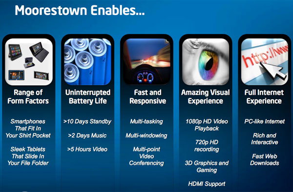
Time sure does fly. Today Intel is finally unveiling its first Atom processors for smartphones and tablets. Welcome to Moorestown.
Craig & Paul’s Excellent Adventure
Six years ago Intel’s management canned a project called Tejas. It was destined to be another multi-GHz screamer, but concerns over power consumption kept it from coming to fruition. Intel instead focused on its new Core architecture that eventually led to the CPUs we know and love today (Nehalem, Lynnfield, Arrandale, Gulftown, etc...).
When a project gets cancelled, it wreaks havoc on the design team. They live and breathe that architecture for years of their lives. To not see it through to fruition is depressing. But Intel’s teams are usually resilient, as is evidenced by another team that worked on a canceled T-project.
The Tejas team in, er, Texas was quickly tasked with coming up with the exact opposite of the chip they had just worked on: an extremely low power core for use in some sort of a mobile device (it actually started as a low power core as a part of a many core x86 CPU, but the many core project got moved elsewhere before the end of 2004). A small group of engineers were first asked to find out whether or not Intel could reuse any existing architectures in the design of this ultra low power mobile CPU. The answer quickly came back as a no and work began on what was known as the Bonnell core.
No one knew what the Bonnell core would be used in, just that it was going to be portable. Remember this was 2004 and back then the smartphone revolution was far from taking over. Intel’s management felt that people were either going to carry around some sort of mobile internet device or an evolution of the smartphone. Given the somewhat conflicting design goals of those two devices, the design team in Austin had to focus on only one for the first implementation of the Bonnell core.
In 2005, Intel directed the team to go after mobile internet devices first. The smartphone version would follow. Many would argue that it was the wrong choice, after all, when was the last time you bought a MID? Hindsight is 20/20 and back then the future wasn’t so clear. Not to mention that shooting for a mobile extension of the PC was a far safer bet for a PC microprocessor company than going after the smartphone space. Add in the fact that Intel already had a smartphone application processor division (XScale) at the time and going the MID route made a lot of sense.
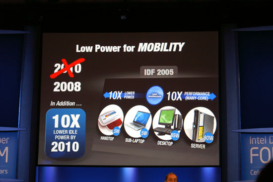
The team had to make an ultra low power chip for use in handheld PCs by 2008. The power target? Roughly 0.5W.
Climbing Bonnell
An existing design wouldn’t suffice, so the Austin team lead by Belli Kuttanna (former Sun and Motorola chip designer) started with the most basic of architectures: a single-issue, in-order core. The team iterated from there, increasing performance and power consumption until their internal targets were met.
In order architectures, as you may remember, have to execute instructions in the order they’re decoded. This works fine for low latency math operations but instructions that need data from memory will stall the pipeline and severely reduce performance. It’s like not being able to drive around a stopped car. Out of order architectures let you schedule around memory dependent operations so you can mask some of the latency to memory and generally improve performance. Despite what order you execute instructions, they all must complete in the program’s intended order. Dealing with this complexity costs additional die area and power. It’s worth it in the long run as we’ve seen. All Intel CPUs since the Pentium Pro have been wide (3 - 4 issue), out of order cores, but they also have had much higher power budgets.
As I mentioned in my original Atom article in 2008 Intel was committed to using in order cores for this family for the next 5 years. It’s safe to assume that at some point, when transistor geometries get small enough, we’ll see Intel revisit this fundamental architectural decision. In fact, ARM has already gone out of order with its Cortex A9 CPU.
The Bonnell design was the first to implement Intel’s 2 for 1 rule. Any feature included in the core had to increase performance by 2% for every 1% increase in power consumption. That design philosophy has since been embraced by the entire company. Nehalem was the first to implement the 2 for 1 rule on the desktop.
What emerged was a dual issue, in-order architecture. The first of its kind from Intel since the original Pentium microprocessor. Intel has learned a great deal since 1993, so reinventing the Pentium came with some obvious enhancements.
The easiest was SMT, or as most know it: Hyper Threading. Five years ago we were still arguing about the merits of single vs. dual core processors, today virtually all workloads are at least somewhat multithreaded. SMT vastly improves efficiency if you have multithreaded code, so Hyper Threading was a definite shoe in.
Other enhancements include Safe Instruction Recognition (SIR) and macro-op execution. SIR allows conditional out of order execution depending if the right group of instructions appear. Macro-op execution, on the other hand, fuses x86 instructions that perform related ops (e.g. load-op-store, load-op-execute) so they go down the pipeline together rather than independently. This increases the effective width of the machine and improves performance (as well as power efficiency).
Features like hardware prefetchers are present in Bonnell but absent from the original Pentium. And the caches are highly power optimized.
Bonnell refers to the core itself, but when paired with an L2 cache and FSB interface it became Silverthorne - the CPU in the original Atom. For more detail on the Atom architecture be sure to look at my original article.
The World Changes, MIDs Ahead of Their Time
Silverthorne lacked integration, which wasn’t a problem for MIDs and netbooks, but it kept the chip out of smartphones. Between 2004 and Atom’s introduction in 2008 the iPhone happened. All of the sudden the clunky MIDs we were reluctantly waiting for stopped being interesting. What we wanted were more iPhones, and iPhone clones. Then came Android and the rest is history. While Atom had tremendous success in netbooks, Intel’s decision to pursue a discrete route first kept it out of smartphones.
Luckily, next on the list after the first Atom was a more integrated one with the goal of dropping power consumption. We saw this with Pine Trail, the netbook Atom that brought the memory controller and GPU on-die. Performance didn’t improve because unlike most integrated memory controllers, this one still connected to the CPU via a FSB.
Intel Atom "Diamondville" Platform 2008 | Intel Atom "Pine Trail" Platform 2009-2010 |
 |  |
Pine Trail still has all of the bells and whistles of a PC platform however. Take the PCI bus for example. Every 12 microseconds it wakes up and polls every IO on the platform. That kills idle battery life, especially when you’ve got a tiny smartphone battery. Pine Trail is useless for smartphones, and that’s where Moorestown comes in.
If you thought this was the netbook Atom squeezed into a smartphone, you’re very wrong. It’s got a completely different memory controller, a true smartphone GPU (the same core, but clocked higher than what’s in the iPhone 3GS) and a ton of power optimizations that just don’t exist in the netbook version. The chipset is also very different. The PCI bus is gone as is anything that could ruin power consumption. Intel did a lot of optimization and a lot of cutting here. What resulted is something that looks a lot like a smartphone hardware platform and nothing like what we’re used to seeing from Intel.
This is Moorestown.
Moorestown: The Two Chip Solution That Uses Five Chips
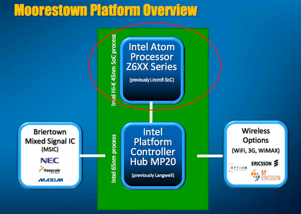
Intel calls Moorestown a two-chip solution. That’s the Lincroft SoC and the Langwell IO Hub. Intel says there’s no architecture limitation for splitting these two up, it was just a way of minimizing risk. You put the bulk of the 3rd party technologies in the Langwell IO Hub and keep the important, mostly Intel controlled components in Lincroft. This is still the first SoC that Intel is going to market with, so splitting the design into two chips makes sense. The followon to Moorestown, codenamed Medfield, will integrate these two once Intel is comfortable.

The 45nm, 140M transistor Lincroft die
Lincroft houses the CPU, GPU and memory controller and is built on Intel’s 45nm process. This isn’t the same 45nm process used in other Intel CPUs, instead it’s a special low power version that trades 6 - 8% performance for a 60% reduction in leakage. The tradeoff makes sense since the bulk of these chips will run at or below 1.5GHz. And by the way, it’s now called the Atom Z600 series.
| Transistor Comparison | |||||
| Intel Atom Z5xx Series | Intel Atom Z6xx Series | NVIDIA Tegra 2 | |||
| Manufacturing Process | 45nm | 45nm | 40nm | ||
| Transistor Count | 47M | 140M | 260M* | ||

Langwell, now known as the Intel Platform Controller Hub (PCH) MP20, holds virtually everything else. It’s got an image processing core that supports two cameras (1 x 5MP and 1 x VGA), USB 2.0 controller, HDMI output (1080p) and a NAND controller that can support speeds of up to 80MB/s. The whole chip is managed by a 32-bit RISC core.
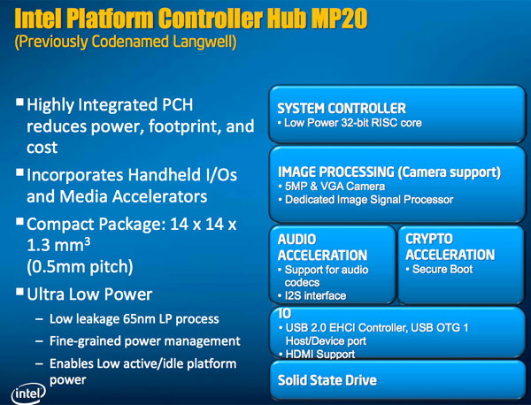
Langwell is a 65nm chip built at TSMC. TSMC has existing relationships with all of the IP providers for the blocks inside Langwell, so making it at TSMC is a sensible move (a temporary one though, with Medfield Intel will integrate all of this).
and_PlatformControllerHub_package2_sm.jpg)
Langwell (left) and Lincroft (right)
While Lincr, err, Atom Z600 and the Intel PCH MP20 are enough for a traditional system, they are not enough for a smartphone. You need wireless radios, that’s one chip for WiFi and one for 3G support. You need something to handle things like power management, charging the battery and controlling the touch screen. That’s an additional chip, called Briertown.


We’re up to four chips at this point, but you need at least one more. While modern day smartphone SoCs ship with on-package memory, Intel doesn’t yet support that. Obviously it’s not impossible to do, Marvell, TI, Qualcomm and Samsung do it with all of their SoCs. Look inside Apple’s iPad and you won’t see any DRAM chips, just a Samsung part number on the application processor package. Intel doesn’t have the same experience in building SoCs and definitely not in integrating memory so it’s not a surprise we don’t have that with Moorestown. Unfortunately this means a smartphone manufacturer will need as many as five discrete chips to support Moorestown.
| Platform Size | |||||
| Moorestown | |||||
| CPU + Chipset | 387 mm2 | ||||
| Total Platform Area | 4200 mm^2 | ||||
| SoC Package Size | 13.8 mm x 13.8 mm x 1.0 mm | ||||
| PCH Package Size | 14 mm x 14 mm x 1.33 mm | ||||
And now we know why Intel has been showing off its extremely long form factor prototype all this time:
Aava to the Rescue: An iPhone Sized Moorestown Platform
Aava Mobile is a smartphone platform manufacturer. It does for smartphones what Pegatron (formerly ASUS) does for notebooks. Aava builds the motherboard and chassis, while the customer adds customization, software and apps.
Aava showed us its Moorestown platform which is about the size of an iPhone 3GS, but a bit narrower and thinner (although longer):
Aava’s reference platform has a 3.7” 800 x 480 OLED display (or an optional 3.8” 864 x 480 TFT display). It weighs 125g, offers 285 hours of standby battery life, 8.5 hours GSM talk time, 5.4 hours of 3G talk time and 5.2 hours of web browsing time using its 1500 mAh battery. Up to 16GB of NAND flash is supported on board.
| Aava Mobile Moorestown Reference Platform | |||||
| Specifications | |||||
| Dimensions with Battery | 118 mm x 56 mm x 11 mm | ||||
| Weight | 125g | ||||
| Standby Battery Life | 285 hours | ||||
| GSM Talk Time | 8.5 hours | ||||
| 3G Talk Time | 5.4 hours | ||||
| Web Browsing Battery Life | 5.2 hours | ||||
| Battery Capacity | 1500 mAh | ||||
| Display | 3.7" OLED 800 x 480 or | ||||
| Multitouch | Capacitive | ||||
| Storage | up to 16GB NAND, micro SD card | ||||
| Camera | 5MP or 8MP Main 2MP Second | ||||
| Wireless | WiFi, Bluetooth 2.1 + EDR | ||||
It’s got a capacitive multi-touch display and supports AGPS, digital compass, accelerometer, proximity sensor, 5MP or 8MP main camera (driven by a separate image processor), 2MP secondary camera, LED flash, FM RDS radio, stereo speaker, stereo mic, stereo headset with answer button and Bluetooth 2.1 + EDR.

It’s a pretty full featured reference platform that would allow companies to deliver a pretty powerful iPhone competitor. As for the OS...
Moblin/MeeGo: The Fastest Smartphone OS?
PC game developers often criticize Intel for holding back the whole industry by not shipping faster integrated graphics. Game developers have to target the least common denominator of graphics hardware, which happens to be Intel’s integrated graphics. So nearly all PC games suffer as a result.
Moorestown is a good bit faster than any ARM based SoC on the market today. Memory bandwidth limitations aside, if you look at our recent Apple A4 vs. Atom performance comparison you’ll see what sort of gap exists between what you get today in a smartphone and what Intel is trying to deliver:
Unfortunately for Intel, all smartphone OSes are optimized for the least common denominator in SoC performance. That is 400MHz - 1GHz ARM11 or Cortex A8 class hardware. Smartphone OS vendors need to make sure their OSes run on the majority of hardware, which just isn’t Moorestown. Intel needs something to take advantage of its added performance, so Intel had to go off and do some software work. Irony is hilarious.
Moorestown is useless if it doesn’t offer significantly better performance or user experience (or both) than its competitors. To ensure this, Intel did two things.
First, Intel bought a company called Wind River. A $400M company prior to acquisition, Intel snagged WindRiver back in July of 2009. Their mission statement? To take open source software and make it commercially viable.
Whether it’s stress testing or adding new features, Wind River takes open source software and improves it to the point where you can now sell it as a commercial product. This is similar to what Apple did with the base of much of OS X. You take some good open source projects and pay people to polish and harden the last 10 - 20% of them.
Wind River has a platform for Android. It incorporates Atom optimizations into Android, hardens the software stack and prepares it for use in Moorestown devices. Google has little incentive to dedicate a lot of support to Moorestown, so Intel had to internalize that.
The second thing Intel did to ensure Moorestown’s performance wouldn’t go to waste was the development of Moblin. A smartphone/tablet targeted Linux based OS, Moblin has been lurking in our minds for well over a year now. I never really got why Intel felt the need to support the development of a mobile OS until now.

Moblin running on Moorestown
Moblin will be the highest performance OS for Moorestown to run on top of. Until a company like Apple or Google decides to embrace Moorestown, Intel needed a way to guarantee an optimized software stack for Moorestown. Moblin is that guarantee. It’s designed from the ground up to be Atom optimized, it’ll be faster than any other OS running on Moorestown and will also do the best integration of power management for Moorestown. Intel knows the architectures of its chips best, and Moblin effectively knows whatever Intel knows.
A Moorestown specific OS could also evolve to include more CPU intensive UIs and features just wouldn’t work well on the majority of ARM devices out there, which would in turn give Moorestown a tangible feature advantage in the smartphone market.
Earlier this year Intel and Nokia announced their cooperative efforts on an OS called MeeGo. Take one part Moblin and one part Maemo and you get MeeGo. The idea is to take Moblin and expand it to more platforms (particularly ARM based devices). Moblin will eventually go away and there will only be MeeGo, however there are currently smartphones and tablets based on both Moblin and MeeGo in development.
While Moblin and MeeGo are the best platforms for Moorestown, there’s a lot of reinventing the wheel that needs to be done. Thus the first Moorestown based smartphones will likely run Android.
The Neutral Role
Carriers aren’t very happy with Apple and Google. They’ve effectively wrestled power away from the carriers and left them as nothing but network providers. In my eyes this isn’t a bad thing. Over the past several years the major carriers have shown us nothing other than they can’t be trusted with too much power. Where there is frustration, there’s money to be made.
Intel wants to capitalize on that frustration by offering the carriers an alternative. Moblin won’t be branded, carriers could customize their own builds and do whatever they want with them. The carriers would ultimately limit what could run on their phones, much like Apple does today. It puts power back in the hands of the carrier, which is something they obviously like.
Whether or not that’s a good thing for the consumer is another question entirely. Intel tells me that the carriers have learned a lot from watching Apple and Google, and that they have no interest in making the same mistakes twice. I’m not sure I believe that just yet.
More OS Support if Needed
Intel made it clear that while it’s only focusing on Android, Moblin and MeeGo at the start, if a vendor were to express interest in doing a custom design around Moorestown the answer wouldn’t be no. In other words, if Apple wanted to move iPhone OS to Moorestown, Intel will make it happen.
Intel also mentioned that Moblin is an enabling necessity for Moorestown. If that need ever goes away, it has no issues handing the market over to Apple, Google or whoever wants to carry the torch. Intel doesn’t want to be in the mobile OS business, it’s simply participating because it is compelled to in order to build the best environment for Moorestown to succeed. If Intel’s plan works out, then all smartphones would eventually use some Moorestown derivative and they would be optimized for much higher performance CPU right off the bat. We’re not there today, so Moblin has a role to play.
There's also the question of Windows 7 support. Without a PCI bus, Moorestown can't run the popular desktop OS. However if Intel were to deliver a version of Moorestown with PCI support, that could solve that problem...
Intel Takes a Stand: No Windows Phone 7 Support
Apparently someone at Microsoft must’ve peed in Intel’s cheerios because Moorestown won’t be found in any Windows Phone 7 devices. According to Intel it’s more than just a spat over breakfast, Intel claims that Windows Phone 7 is still optimized for very low end ARM SoCs. Intel went on to say that despite the advances in the OS, Windows Phone 7 isn’t progressing fast enough from an architecture standpoint and that it is an “old OS with many of the warts we’re trying to get away from”. Apparently Windows Phone 8 falls into the same category and it too will not be supported by Moorestown.
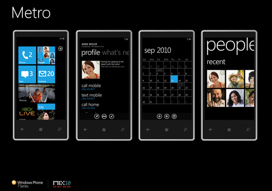
Windows Phone 7, Not Supported by Moorestown
The same goes for Symbian (obviously).
Intel says that these OSes aren’t on a steep enough roadmap to make the Moorestown investment. It’s difficult to say whether or not Intel is right, we’ll have to wait to see how Windows Phone 7 scales with performance once the first devices hit later this year.
x86 Everywhere: Two Years Later
In my original Atom architecture article I spoke about the benefits of having a platform that could run existing applications, in this case x86 applications. Developers don’t like porting to new hardware, which is one reason GPU computing hasn’t really taken off yet.
Since then we’ve seen a major change: the introduction of platform specific App stores. Starting with the iPhone App store and extending to most smartphone platforms (Android Marketplace, Palm App Store), with a simple way to sell their apps we’ve seen a completely new group of developers emerge specifically targeting smartphones. These aren’t your traditional developers. Companies like Adobe and Microsoft are effectively absent from any of the app stores. Instead what you find are smaller development houses putting forward smaller but very useful applications and games for use on these smartphones.

The scariest part for Intel is that none of these apps run on x86 hardware. While there are still more x86 applications than iPhone or Android apps, there are more smartphone friendly apps running on ARM architectures than x86. The advantage of being able to run existing code without lengthy port times just isn’t an advantage today. In fact, you could consider the move to x86 a disadvantage from the perspective of a company like Apple or Google. While it’d be simple to offer x86 versions of apps through a closed store system, it means extra work for the developer and for Apple with little benefit today. By aiming at the netbook first, Intel may have squandered one of its major potential advantages in the smartphone.
All isn’t lost however. There’s still the argument that the applications and algorithms that have yet to be moved to smartphones still exist in x86 form. As smartphones grow more powerful, so will the types of things we try to do on them.
The Memory Controller: 32-bit LPDDR1
The Lincroft SoC (or Atom Z600) measures 13.8 mm x 13.8 mm x 1.0 mm. That’s smartphone SoC sized. In order to hit the small package size and in order to keep power consumption down, the single channel DDR2 memory controller from the netbook Atom is gone. What we have instead is a 32-bit wide LPDDR1 memory bus capable of supporting up to 1GB of memory. At 400MHz that’s about the amount of memory bandwidth we had on PCs 10 years ago.
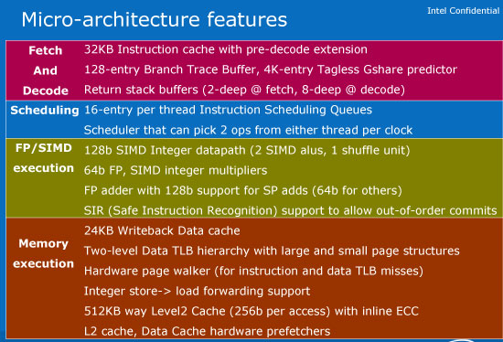
Intel claims that the majority of workloads on smartphones are compute and not memory bandwidth bound so the reduction in memory bandwidth isn’t going to be an issue. Lincroft's caches are the same as Silverthorne before it (24/32KB L1 + 512KB L2).
Compared to smartphone SoCs today, Intel isn’t really outgunned:
| 2010 Application Processor Comparison | |||||
| Memory Interface | |||||
| Apple A4 | 32-bit LPDDR1/LPDDR2 (?) | ||||
| Intel Atom Z600 | 32-bit LPDDR1 | ||||
| TI OMAP 3430 | 32-bit LPDDR1 | ||||
| TI OMAP 4430 | 2 x 32-bit LPDDR2 | ||||
| NVIDIA Tegra 2 | 32-bit LPDDR2 | ||||
| Qualcomm Snapdragon QSD8250 | 32-bit LPDDR1 | ||||
It’s only next year when products based on TI’s OMAP 4430 chip that we’ll see a real ramp in memory bandwidth. Intel will offer a version of Lincroft for tablets with a 32-bit DDR2-800 interface. It can support a maximum of 2GB of memory.

The Lincroft memory controller has less bandwidth than the netbook version, but it's more efficient as a result. Intel included a lot of optimizations, particularly for graphics to improve bandwidth utilization.
Clock Speeds: 1.2GHz - 1.5GHz for Smartphones, 1.9GHz for Tablets
Intel isn't announcing individual Atom Z600 SKUs just yet, but we do know that all versions of the chip will support Hyper Threading (likely due to maintain a performance advantage compared to upcoming dual-core ARM offerings). There will be two versions of the Atom Z600 chips, one for smartphones and one for tablets.

The smartphone SKUs will run between 1.2GHz and 1.5GHz, while the tablet version of the Z600 will run at up to 1.9GHz.
Power Management: Clock Down or Turbo Up
Eleven years ago Intel demoed a technology it called Geyserville for mobile CPUs. The technology simply ran the CPU at a lower frequency when running on battery power and a higher frequency when plugged in. Intel eventually called this SpeedStep.
Four years later we got EIST, Enhanced Intel SpeedStep Technology. This allowed a mobile (and eventually desktop) CPU to run at any frequency depending on the performance demanded by the OS and the running applications.
On today’s Atom processors this usually means the chip will run as low as 600MHz when idle and at 133MHz increments all the way up to 1.66GHz under load. You don’t normally drop below 600MHz because that falls into the inefficient range of CPU performance scaling for a netbook/nettop. In a smartphone though, the majority of time your CPU isn’t being used. The SoC and accessory processors have enough custom logic offload a lot, even when your phone isn’t idle.
Lincroft, or the Atom Z600 series, supports even lower frequency modes. The CPU can clock itself down well below 600MHz.
When you need performance however Lincroft has something similar to Turbo Boost on Intel’s desktop CPUs. On the Atom Z600 series it’s called Burst Mode and unlike Turbo, it is more tightly integrated with the OS.
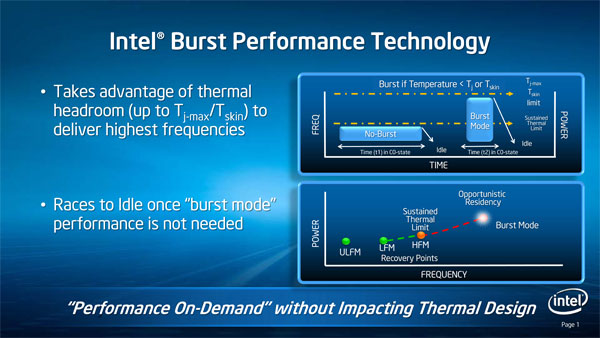
EIST and other dynamic clocking technologies rely on OS P-states to determine what frequency the chip should run at. If an OS requests P0, the CPU simply runs at its highest frequency.
On the Core i5 and i7, if the OS requests the CPU be in P0, then as long as the chip doesn’t violate any current or TDP limitations it will run at a higher turbo frequency instead of the default maximum clock speed the OS is requesting. P0 will always return the highest possible frequency given the thermal conditions of the chip.
The Atom Z600 doesn’t work like this. All potential burst mode frequencies are enumerated as P-states by the BIOS. An OS with proper support for Moorestown will be able to request any specific clock frequency, even burst frequencies. Loading a web page for example might result in the OS asking for the highest possible burst mode frequency, but while you’re reading the page the OS might request a slower P-state. The chip will run at whatever the OS requests, but it will exit burst mode if the chip’s temperature gets too high.
The FSB speed also scales with clock frequency. Once you reach a certain clock speed threshold, the Atom Z600 will automatically double its FSB frequency to help feed the CPU faster. The goal isn’t just to deliver peak performance, but it’s also to complete tasks faster so that the SoC can return to an idle state as soon as possible. The hurry up and go idle approach to mobile CPU performance has been one of Intel’s basic tenants for well over a decade now. And it does work. This is the reason we’ve generally seen an increase in battery life from each subsequent version of the Centrino platform.
The software management of burst mode puts more emphasis on the OS and platform vendors to properly tune their devices for the best balance of performance/power consumption. You can see why Wind River’s Android platform and Moblin are necessary to get the most out of Moorestown.
Power Gating
Until the Atom Z600 series, the only Intel CPUs to power gate were the Nehalem/Westmere derived chips. In Moorestown, everything is both power and clock gated.
The CPU itself has its usual power states; C0 implies full power, full performance, and C6 is a deep sleep state where power is shut off to the entire CPU and state is saved in a small amount of active SRAM. There’s finer grained clock and power gating in Lincroft than in Intel’s Core i7.

Moorestown is a SoC platform however, so we need some new power states. Intel calls them S0i1 and S0i3. As with CPU power states, the higher the number, the more that’s shut off.

Virtually all blocks in Lincroft and Langwell are clock and power gated. In S0i1, everything from the CPU and GPU to interconnects are power gated. From the sounds of it, S0i1 is where you’d find your smartphone if you just left it on the table for a few seconds. The display would shut off and all internal components would be power gated. Pick it back up, hit a button and you get pretty quick recovery.
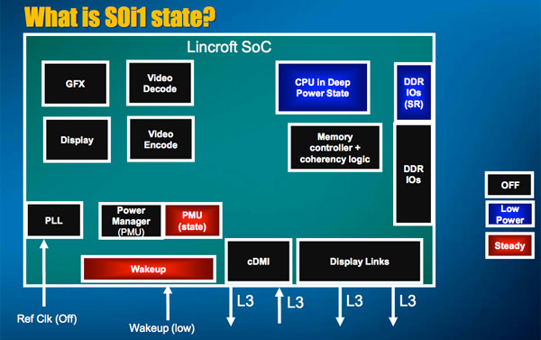

S0i3 however completely powers down virtually all components and keeps a small amount of SRAM active with state data. This is the phone locked and in your pocket state.
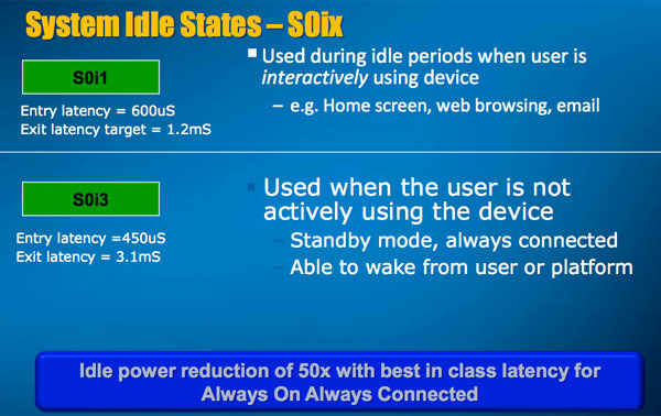
Getting out of these power states is relatively quick. S0i3 takes around 3ms while S0i1 takes 1ms.
The impact of these idle states is huge. On a reference Moorestown platform (this includes the Moorestown chips, display, 3G radio, basically a fully functional phone), Intel measured total platform power in S0i3 at 21 - 23mW. That’s a ~50x reduction compared to Menlow, and that’s what makes Moorestown suitable for use in a smartphone.
OS Driven Power Management
When Intel introduced Nehalem and the Core i7, we saw a new generation of power engineering in microprocessors. In the past, the OS would request a particular performance state from the CPU and the chip would respond by changing its clock speed. Nehalem’s Power Control Unit (PCU) instead dedicated enough transistors to build a 486 to monitoring the power and performance demands on the chip. Based on those demands and what the OS was doing, the PCU would power up or down individual cores, as well as move clock speeds up or down. The PCU would guess at what the OS was trying to do and respond accordingly.
Nehalem and its successors were massive chips, eating up to 130W of power under load and idling down in the 6 - 10W range. Lincroft has to be sub-1W under load and 6mW at idle. With even more stringent power demands and a much smaller die, Intel couldn’t blow a sizeable percentage of the Lincroft transistor budget on power management.
Instead of guessing at what the OS wants, the Moorestown platform uses OS Driven Power Management (OSPM) to tell Lincroft and Langwell what to do. OSPM is supported in Moblin and presumably the Wind River build of Android.

The OSPM process tells the hardware what apps it’s running and to shut down what it doesn’t need. There are well defined operating modes - standby, internet browsing, MP3 playback, video playback, voice call, video capture, etc... Based on the profile, the hardware doesn’t have to guess at what it should turn off/on, it just does it right away.
The OSPM driver communicates directly with the two power management units in Moorestown - one in Lincroft and one in Langwell. It instructs those PMUs to shut off various blocks, and in turn they tell Briertown to gate and cut voltage to the parts of chip that aren’t needed.

I wondered if this couldn’t be done in hardware, but it seems that given current die constraints and the sort of accuracy of information it needs Intel must implement at least some of the power management control in software. Toolkits will be available for developers to control the OSPM.
Putting Power in Perspective: Estimated Battery Life of a Moorestown Phone
I wanted to get Moorestown hardware in time for the launch but unfortunately nothing is quite ready yet, so we’ll have to rely on Intel’s data.
As I just mentioned, Intel expects a Moorestown phone to idle at 21 - 23mW. Paired with a 1500mAh battery that’s 10 days of standby time. Intel claims that Snapdragon phones idle at 25mW. If that’s true then Moorestown is competitive.
Audio playback is expected to consume around 120mW of power (for the entire platform, not just the silicon). Intel estimates that’ll get you around 48 hours of continuous music playback. Intel was quick to add that this is better audio playback battery life than anyone else on the market today, although both TI and NVIDIA are promising better battery life than that with their next-generation SoCs (OMAP 4430 and Tegra 2).
| Moorestown Battery Life (Figures by Intel) | |||||
| Total Phone Power Consumption | |||||
| Idle | 21 - 23 mW | ||||
| Audio Playback | 120 mW | ||||
| 1080p Video Playback | 1.1W+ | ||||
| Web Browsing (WiFi) | 1.1W | ||||
| 2G Phone Call | 550 mW | ||||
| 3G Phone Call | 1.2W | ||||
Intel’s video playback estimates are lower than the competition, Moorestown is expected to only provide 5 hours of continuous HD video playback compared to 10 hours on an iPhone 3GS. That comes from 1.1W+ platform power consumption during video playback.

Intel estimates that Moorestown based devices will last about 5 hours when browsing the web on WiFi. Talk times are expected in the 4 - 5 hour range over 3G, and 8 - 10 hours on 2G.
If these numbers hold true in shipping Moorestown devices, I’d expect to see anywhere from iPhone to iPhone 3GS levels of battery life. Audio decoding seems good, while other aspects like video playback aren’t so great. Web browsing power consumption really varies based on the test. I measured power consumption on my iPhone 3GS and saw 1.1 - 1.3W while loading the AnandTech front page. That would imply Moorestown platform battery life could be competitive.
As soon as I can get my hands on some actual hardware I plan on verifying all of this data myself. Intel claims that the top 5 handset manufacturers see power consumption in the 750mW - 1.5W range, so Moorestown should find itself right in the middle of all of them.
The Intel GMA 600 by Imagination Technologies
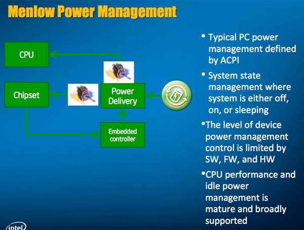
The iPhone 3GS, iPad, Motorola DROID and Palm Pre all use Imagination Technologies’ PowerVR SGX mobile GPU. The SGX 535 running at 200MHz was used in Poulsbo, the North Bridge used in the very first Atom MID platform (Menlow). That was a 130nm chip. Intel called it the GMA 500.
Moving the GPU core on-die shrunk it considerably. At 45nm it should occupy roughly 1/8 - 1/10 the space of the GPU at 130nm). The PowerVR SGX 535 in Lincroft can also run at up to 400MHz, although it’s up to the handset vendors themselves to pick the right balance of clock speed vs. power consumption. It’s also possible that different versions of the Atom Z6xx line will have different GPU clocks. The new GPU is called the Intel GMA 600.

To the best of my knowledge all current smartphone implementations of the PowerVR SGX 535 run at 200MHz. This should give Intel the leg up in graphics performance should a vendor choose to run the GPU at such a high clock rate. It’s difficult to tell what impact we’ll see on battery life.
The Display
Lincroft only supports two display interfaces: 1024 x 600 over MIPI (lower power display interface) or 1366 x 768 over LVDS (for tablets/smartbooks/netbooks). 1080p HDMI out is supported Langwell.
Video Decoding Support: H.264 High Profile at up to 20Mbps
Imagination Technologies is also on tap to produce the video decoding hardware used in Lincroft. The PowerVR VXD is also used in the iPhone 3GS and the iPad, it’s here in Moorestown as well.
The implementation in Moorestown, combined with Intel’s caches and memory controller can apparently support 1080p H.264 base, main and high profile content at up to 20Mbps. At 1.1W platform power during video playback, that’s pretty impressive.
Video encoding is supported for the first time, also using ImgTec IP (PowerVR VXE). You get up to 720p30 H.264 base profile L3 video encode with Moorestown. You won’t see 1080p encode support until Medfield.
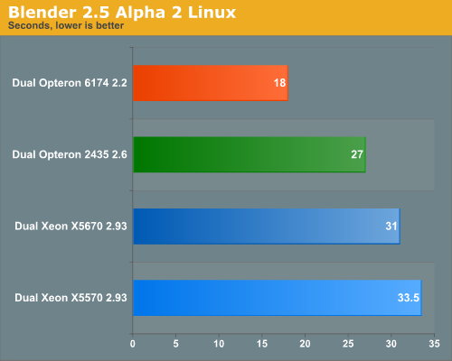
CPU Performance: Moorestown Rocks?
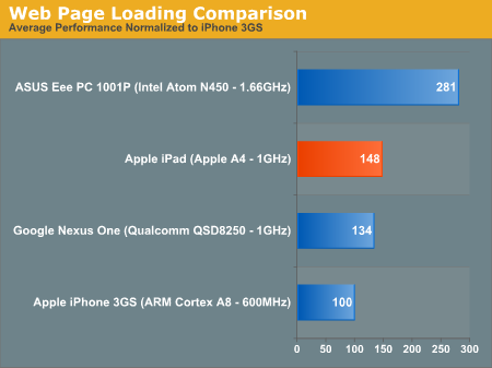
In my iPad review I pointed out the huge gap between the performance of today’s 1GHz smartphone SoCs and an Atom powered netbook.
It’s impossible to estimate the performance of Moorestown without functional hardware, but we can assume that it’s somewhere in between the ARM based SoCs and the netbook in the chart below.
Intel provided some SPECint numbers comparing Moorestown to various smartphone application processors shipping in 2010 (either now or later). Keep in mind that SPECint is just as much of a compiler benchmark as it is a hardware benchmark, so real world performance could very well differ. We won’t know how well Moorestown stacks up until we can evaluate it ourselves. But if Intel’s numbers are even remotely accurate, this is the sort of leap in performance we honestly need in the smartphone space:
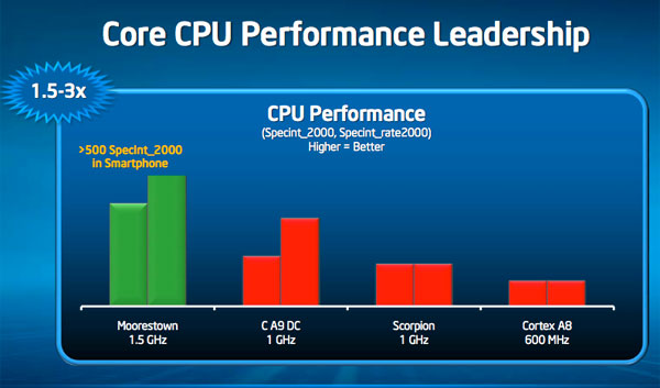

The slowest member of the Atom Z600 series will run at 1.2GHz, the fastest (for smartphones) will run at 1.5GHz. While multithreaded performance on a dual Cortex A9 at 1GHz approaches that of a 1.2GHz Moorestown, nothing can touch the 1.5GHz part. Single threaded performance is just as impressive.
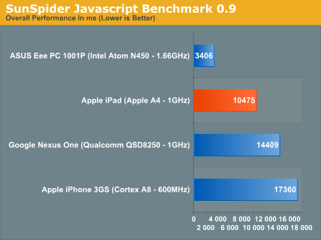
The Sunspider score is super impressive as well. Intel is posting a sub-2s Sunspider score, the best we've seen thus far on a ARM based platform is ~10 seconds on the iPad:
These numbers are from Intel so we have to take them with a grain of salt. And as I already mentioned, we’re looking at pure CPU/compiler performance here - real world application performance is a different story entirely. But it’s a safe bet to assume that Moorestown will at least be faster than any application processor on the market today.
A high clocked dual Cortex A9 could give it a healthy challenge though.
GPU Performance: Moorestown Rules?
Intel provided three numbers to instill confidence in Moorestown’s graphics capabilities. The first was a claim of over 100 fps running Quake 3. I saw this in person so I can confirm that you can actually run a timedemo of Quake 3 at above 100 fps on Moorestown. NVIDIA claims over 40 fps on the Tegra 2 at 720p with AA, but it’s unclear how comparable these numbers are.
The next two numbers are from 3DMark Mobile ES 2.0 using the Taiji and Hoverjet benchmarks:

This is comparing the performance of Moorestown to the lower clocked SGX 535 among other GPUs. The performance improvement is more than 2x.
Again, these came from Intel directly so we can’t vouch for their applicability to the real world.
Availability and Medfield
We got Menlow in 2008. Intel promised Moorestown in 2009/2010. The chips are done, but you won’t see products until the second half of this year. We’ve actually seen Moorestown reference designs at this point so it’s safe to say that we’ll see some devices before the end of the year, but perhaps the most exciting ones won’t appear until later.
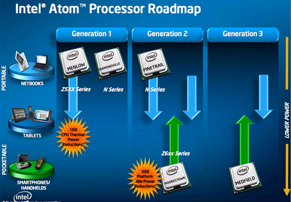
In 2011 we’ll meet Medfield. A 32nm shrink of Moorestown that combines Lincroft and Langwell into a single SoC. Medfield will double graphics performance, triple imaging capability (higher MP cameras) and bring full HD encode/decode (Blu-ray on my phone?). A reduction in chip count will mean even smaller form factors, while the move to a single 32nm SoC (rather than 45nm + 65nm) should give us longer battery life for idle, video and web browsing. Things like talk time are more a function of the modem than anything else. When you’re on a call the majority of Intel’s components are almost completely powered down, it’s just the modem and its friends that are sipping power.
Medfield is apparently on track, it’ll be in production next year and Intel told me not to expect any more updates on Medfield until the second half of 2010.
Final Words
This isn’t your netbook’s Atom. Thanks to an incredible amount of integration, power management and efficiency Moorestown has the potential to be the most exciting thing to hit the smartphone market since the iPhone. If Intel can deliver a platform that offers greater than 2x the performance of existing smartphones in the same power envelope it has a real chance of winning the market.
The problems are obvious. Intel is the underdog here, it has no foothold in the market and the established OSes are currently very ARM optimized. Not only does Intel have to get Moorestown off the ground but it also needs a win on the software side as well. MeeGo has to, er, go somewhere if this is going to work out. The one thing I will say is that the expected rarely pans out. The smartphone market in 5 years won't look like an extension of what we see today. Apple and Google dominating the market and running ARM processors is where we are today, I'm not convinced that's where we'll be tomorrow.

Intel's Sean Maloney, heir apparent to the CEO throne, said that to succeed Intel needs 3 out of the top 5 handset guys and a bunch of alternative players. He added, "we feel like we're in good shape for that." In the next 12 - 18 months we should see that come to fruition.
For me however it's more about software and design wins. Intel needs to be in an iPhone, or at least something equally emotionally captivating. It needs a halo product. I believe Intel has the right approach here with Moorestown. To be honest, I've seen the roadmap beyond it and it's very strong. The technology is there. We just need someone to put it to use and that's the part that isn't guaranteed.