Somehow I’d managed to dodge meeting with Globalfoundries since the company was formed earlier this year. For those of you who don’t know, AMD is now officially a fabless semiconductor. AMD provided its two existing fabs to the new company and its partner, ATIC (Advanced Technology Investment Company) provided $6B. ATIC owns 65.8% of the new company and AMD owns the rest, although the two share voting rights.
AMD’s biggest limitation has always been capital. Intel currently has four fabs that will be producing 32nm chips by the end of 2010, AMD currently has (err, had) a single 45nm fab in Dresden. There’s simply no way AMD could compete in the fab game with Intel, so it chose to partner up with ATIC, take $6B of their dollars, and spin off its fab business.
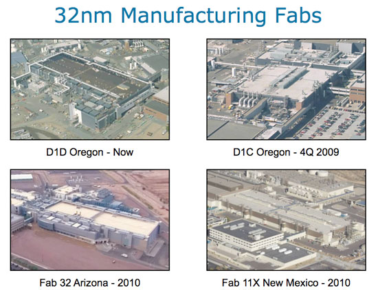
Intel's 32nm fabs for 2010
Until this morning, Globalfoundries only had a single customer - AMD, but that just changed with the announcement that STMicro would be using their fabs. Currently Globalfoundries only has AMD’s two fabs in Dresden, Germany, only one of which is producing modern 45nm SOI wafers. But that too is about to change.

Ceremonial shovels, at a ceremonial ground breaking
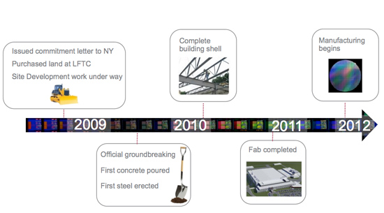
My first official meeting with GF came just this past week, in Saratoga County, NY. That’s the site where its brand new post-AMD fab will be constructed and it’s sort of a big deal. I was there for the ceremonial ground breaking, but concrete doesn’t get poured until September, the shell won’t be finished until 2010 and the fab won’t be done until 2011. Globalfoundries won’t be able to ship revenue generating wafers until 2012. But that’s ok, with $6B in the bank and a strong commitment from wealthy ATIC the company couldn’t be in a better place.
On Competing with TSMC
AMD couldn’t last competing in the foundry game with Intel. The chart below just shows how expensive it gets:
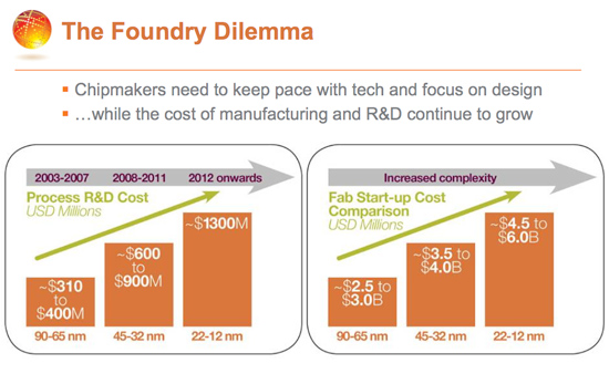
At 32nm a single fab can cost $4B and in just two years it’ll need to be upgraded (to the tune of around a billion) to support 22nm production. For AMD to support the costs alone and remain competitive with Intel, it would have to virtually own the x86 microprocessor market. Even when AMD held the technology crown, that didn’t happen.
The other alternative is to subsidize the cost of these expensive factories over multiple customers. This is where things get interesting. AMD alone may not be able to fill a fab and make the investment pay off, but AMD + Sony + Toshiba + NVIDIA + etc... can definitely make it work.
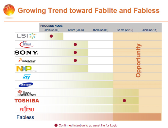
Globalfoundries' potential customers and when they plan on going fabless
Currently, fabless semiconductor manufacturers like NVIDIA (and the graphics division of AMD) go to foundry companies like TSMC for their manufacturing needs. In return, they get nearly the latest manufacturing processes (TSMC is at 55nm for volume and 40nm while Intel is at 45nm moving to 32nm) and don’t have to worry about building expensive fabs.
There are problems with this approach. For starters, TSMC has been having troubles moving to 40nm - as you may have heard. Just as important, you don’t get the most advanced manufacturing process technically available. There’s also the fact that TSMC has very little real competition in the industry; all of the GPUs you’re used to reading about are made at TSMC.
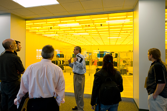
The machine to the left of the man's head in the center of the pic is a 193nm lithography machine. We weren't allowed to take close photos, but that machine costs around $75M. Fabs are expensive.
Companies like Sony, Freescale, Samsung, Toshiba and TI all currently fab their own chips. These chips are far less complex than a Nehalem or a Radeon HD 4890 and are thus made on 130nm, 90nm or 65nm processes. The SoC (System on Chip) in the iPhone 3GS is built on a 65nm process by Samsung at its own fab. Being able to move to 45nm or 32nm alongside Intel would give Apple, Samsung and even ARM in general a tremendous competitive boost in the market place. A 45nm iPhone 3GS would use less power or even run at higher clock speeds.
The need for a modern fab partner increases as you look at Intel’s motions towards competing in the smartphone space. Once Atom finally makes its way into smartphones, Intel could have a manufacturing advantage over the ARM partners - allowing for quicker scaling to lower power and higher performance designs. In other words, companies making smartphone SoCs need a good foundry option to compete with Intel.
The Roadmap
There’s clearly a need for a company like Globalfoundries, even if just to keep TSMC on its toes (hooray competition). But then reality sets in, Global isn’t much of a TSMC competitor yet - it still only has one fab producing 45nm silicon and only SOI at this point.
Here’s what Globalfoundries plans on doing with its existing fabs:
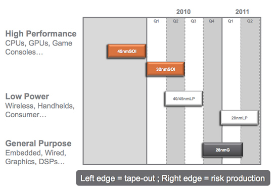
In the second half of 2010 Global will move one of its Dresden fabs to 32nm SOI production for AMD’s CPUs. I’m not expecting anything else to be made on this process other than AMD CPUs at this point.
We’ll see a “low power” 40/45nm process come out of Dresden near the end of 2010 as well. This will actually be for GF’s first non-AMD customer: STMicro.
The real transition happens in 2011, when Global upgrades its older Dresden fab to support 28nm bulk silicon production. Globalfoundries views 28nm as the transition point for many potential customers. It’s not that there’s anything magical about 28nm, but many companies currently have designs for TSMC’s 40nm process and it makes little sense to redo them for manufacturing at Globalfoundries. At 28nm they can simply design for Globalfoundries’ process from the start.
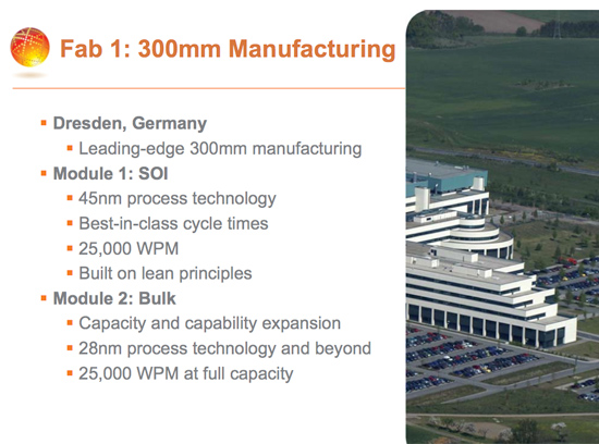
The fabs formerly known as Fab 30 and 36
Note that this 28nm process is a “half-node” (between 32nm and 22nm) and where I’m expecting to see ATI (and NVIDIA) GPUs made at Globalfoundries. The current 40nm products are being made at TSMC but it’s possible that we’ll see the next-generation pitched to GF. The first hybrid CPU/GPU from AMD will be built on GF’s 22nm SOI process in 2012.
Bulk vs. SOI
Back in 2001 AMD started to move to SOI (Silicon on Insulator) for its CPU manufacturing. The benefits of SOI were lower power and faster switching rates, although it came at a higher manufacturing cost. AMD will continue to use SOI for its high performance CPUs because their price can justify the additional manufacturing cost. More price sensitive markets don’t need the performance benefits of SOI and would rather not deal with the price penalties of it either; for those companies Globalfoundries needs to provide a bulk silicon process and in 2010, they will get just that.
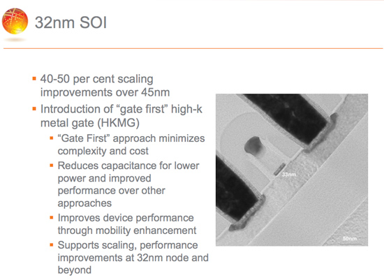
Enabling SOI as well as bulk silicon manufacturing isn’t all that difficult but it does require some work. The first bulk process in Dresden will be a 40nm low power process out of Fab 1 Module 1. The first customer? Not AMD, but rather STMicro. These are the folks who used to make the old Kyro graphics cards, but obviously they’ll be making low power SoCs here instead.
In 2011 Global will offer a 28nm LP bulk process as well as a 28nm general purpose bulk process. The latter will be used for GPUs and other non-ultra-low-power devices.
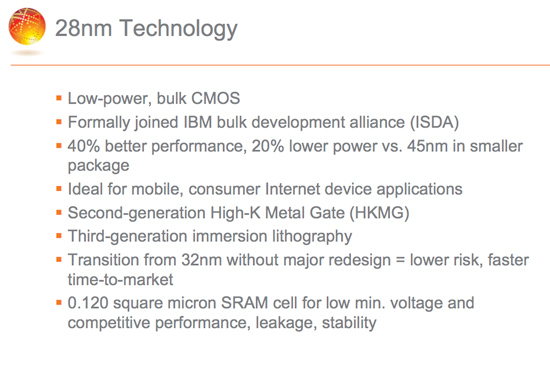
Again, all of these plans involve AMD’s old fabs in Dresden, Germany (formerly Fab 36 and Fab 30, now Fab 1 Modules 1 and 2). Once 2012 rolls around, there will be a new player in town.
Meet Fab 2
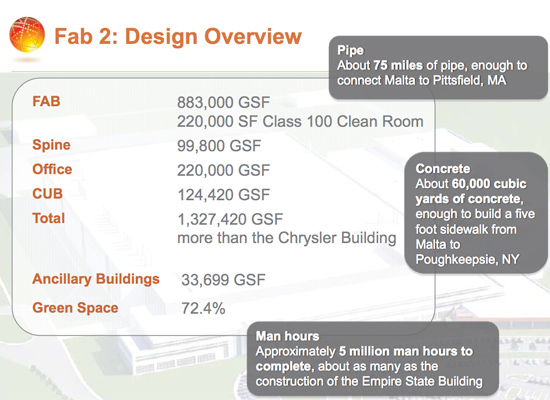
Let’s get the numbers and politics out of the way. Fab 2 will be built in Saratoga County, NY. The plant will cost $4.2 billion to complete, but with the deep pockets of ATIC and tax incentives from the state of NY, this won’t be a problem. When it’s finished you’re looking at more than 1,400 high skilled jobs. It’ll take a couple thousand construction workers to build the place and when it’s all done Globalfoundries is estimating 5,000 ancillary jobs (gotta feed the engineers and entertain their families). Globalfoundries is also contributing $5M to community projects to the two towns that border the Luther Forest Technology Park where Fab 2 will be built. In short, there’s a lot of money going around.

The location actually makes a lot of sense. Just a few miles away is the College of Nanoscale Science and Engineering, a part of the University at Albany. CNSE is not your normal graduate campus; the $4B campus actually houses a modern microprocessor fab facility capable of producing 300mm 45nm wafers just like the best Globalfoundries has to offer today. While the plant is purely a research fab (limited to 25 wafers per day vs. ~1200 per day at Fab 2), it’s serves its purpose for companies and students looking to perform research at an advanced microprocessor fab. CNSE also holds one of the two alpha EUV lithography machines in the world; EUV lithography will be needed to replace immersion lithography to scale down beyond 22nm.

That's where Fab 2 will go
When Fab 2 comes on line in 2012 it'll be a 28nm/22nm fab, with the bulk of its production hopefully being 22nm.
Half vs. Full Nodes
I asked Globalfoundries a question that I'd always wondered for myself: why are GPUs manufactured on half nodes and CPUs manufactured on, er, whole nodes? Let me give you an example.
Intel's CPU transitions went from 90nm to 65nm to 45nm and are now moving to 32nm. AMD followed a similar path.
NVIDIA's GPUs however went from 90nm to 80nm to 65nm to 55nm to 40nm in roughly the same time period. ATI's GPUs did the same.
The in-between nodes (80nm, 55nm and later 28nm) are called half-nodes. And the CPU guys don't use them simply because their design cycles are longer and more complex than what comes out of ATI/NVIDIA. There's no technical downside to using half nodes, it's just added design work for little benefit for a CPU maker.
GPU design cycles are much shorter, so taking advantage of half nodes just makes sense. It all stems from the birth of the 6 month product cycle back in the late 1990s
Maintaining Moore's Law
Every two years we need the ability to make chips smaller and cram more transistors into the same area. It makes microprocessors faster, more complex and cheaper depending on what you do to them. It also really helps with the whole ridiculous pace of innovation our industry likes to maintain.
If our ability to do that came to a halt, we'd be faced with our own little economic-depression in the microprocessor industry.
The threat that it will come to a halt is real, just as the confidence that we'll be able to innovate through for the next 10 - 15 years at least. It's all a matter of size. In order to cut transistor area in half every two years, you need to be able to physically design circuits that small - which requires some very expensive and precise equipment.
Hitting 45nm was difficult, but possible. AMD/Globalfoundries resorted to immersion lithography to make the transition. Basically it involves using liquid to improve the resolution of current 193nm lithography tools. By the time 32nm rolls around, Intel may have to do the same. Scaling beyond 32nm may reach the optical limitations of the current tools. Designing smaller, more densely packed chips may not be possible.
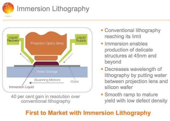
The replacement technology is something called extreme ultraviolet lithography. It's uses 13.5nm wavelength light (instead of 193nm) to be able to realize much finer patterns than current lithography tools.
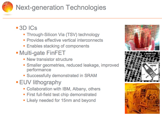
Multi-gate transistors are also expected to be needed at or after 22nm to maintain the sort of progress we've been used to. Multi-gate transistors are also non-planar so you can physically fit more in the same area, helping density issues.
Remember die-stacking? That's coming too.
Final Words
When AMD announced that it would be spinning off its fabs it was honestly the only decision the company could have made. Even while continuing to hemorrhage money after the announcement, the move has the potential to succeed just like the ATI acquisition did; it'll just take a while.
A leaner AMD, focused almost entirely on design and not on keeping fabs full is a better match for Intel. AMD could never compete on manufacturing alone, but at least this way it has the opportunity to compete on technical design.
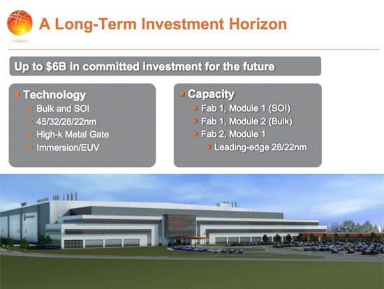
Decoupling manufacturing from microprocessor design wouldn't make sense without the help of ATIC. The $6B investment is enough to give Globalfoundries the chance to start and succeed. AMD simply wouldn't be able to do this without ATIC.
As an independent entity, Globalfoundries itself can do quite well. Microprocessors are becoming increasingly important in the world. The demand for tons of cheap, high performance, low power SoCs and microprocessors is supported by what we've seen happen with smartphones and netbooks. The trend is going to continue and while I'm sure we'll see only a couple of SoC makers dominate the market in the end, they will need a place to make their chips.
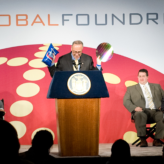
Upstate NY used to be known for making potato chips, now it'll be known for making computer chips. Clever.
The impact of all of this on the US and NY economies is pretty huge. It's all pretty sweet. Over the next three years a $4B building gets created, which means jobs for construction workers, additional revenue for everyone who makes the things buildings are made out of and eventually extra revenue for companies that make microprocessor manufacturing tools. Then, once the building is complete, you get a plant of 1400 people. Many of them are highly skilled workers, their total yearly salary being $88M. Their families move into the area, everyone buys homes or rents apartments, they all shop, eat out, go to movies and the entire local economy benefits.
Of course you have to feed the plant with new hires and luckily there's a big nanotech school graduating really smart folks a few miles away. They now have a place to work and the school has another very appealing employment path to offer its students, attracting even more to its campus.
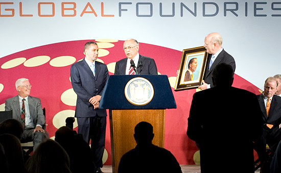
NY's Governor David Paterson and Hector Ruiz. The fab deal is quite political.
All of this from a single fab being made in upstate NY. Did I mention that there are two more spots to build fabs next to Fab 2 Module 1? The rumor is that ATIC wants the next one built in Abu Dhabi though (after all, that is where the money for all of this is coming from).
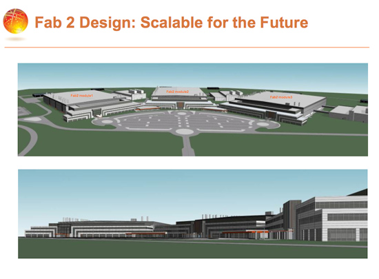
With money in the bank we won't have to worry about Globalfoundries lasting through the recession. Now it's a matter of who the next customers will be.


No comments:
Post a Comment