The most comprehensive coverage and review, enjoy it!
Prologue
Because designing GPUs this big is "fucking hard"
-NVIDIA's VP of Product Marketing Ujesh Desai on GF100
Fermi/GF100/GTX400 has been a long time coming. For an industry where the major players are usually in lockstep with each other in some fashion, this latest cycle has been distinctly out of sync. In September of 2009 we saw AMD launch their Radeon 5000 series, and spend the next 6 months as the performance leader for the discrete graphics market for virtually every price point. NVIDIA on the other hand missed the latest cycle by a mile, and when AMD was delivering 5000 series cards NVIDIA could only talk about the High Performance Computing applications of their next GPU, Fermi. It would be the next big thing, both figuratively and literally.
In January we got the next piece of the Fermi story at CES, when NVIDIA was willing to talk about the gaming-oriented hardware and applications of the first Fermi GPU: GF100. We found out it would be significantly different from the GT200 GPU powering NVIDIA's GTX200 series, that NVIDIA was going to break up the traditional fixed-function pipeline and at the same time take a particularly keen interest in tessellation. What we didn't find out is when it would ship.
Much of this has been in NVIDIA's hands – some of it has not. What's indisputable is that TSMC, the chip foundry used by both AMD and NVIDIA, was not delivering the kind of yields on their 40nm process that AMD and NVIDIA were expecting. Both of them suffered for it. AMD could not get enough viable chips to meet demand for their 5000 series part, leaving a wake of disappointed gamers who could not get AMD's latest wonder, and limiting AMD's ability to profit from one of the few times in AMD/ATI's history where the company had a clear lead over NVIDIA, and if you ask AMD also limiting their ability to control prices. NVIDIA meanwhile had to deal with the fact that they were trying to produce a very large chip on a low-yielding process, a combination for disaster given that size is the enemy of high yields.
What's also indisputable is that this 6 month wait has benefited few people. For the observers of an industry where the competition is cut-throat we saw GPU prices rise, when in the last generation AMD and NVIDIA knocked upwards of hundreds of dollars off of each other's prices practically overnight. It may have been good times overall for AMD, but for buyers the competitive marketplace is sorely missed.
That brings us to today. We can see the light at the end of the tunnel, the end of NVIDIA's 6 month journey is near. We've told you about the compute applications of Fermi, we've told you about the gaming applications of Fermi, and now at long last we can tell you about the first products. It's time to say hello to the GTX 400 series.
Meet the GTX 480 and GTX 470
| GTX 480 | GTX 470 | GTX 295 | GTX 285 | 9800+ GTX | |
| Stream Processors | 480 | 448 | 2 x 240 | 240 | 128 |
| Texture Address / Filtering | 60/60 | 56/56 | 2 x 80 / 80 | 80 / 80 | 64 / 64 |
| ROPs | 48 | 40 | 2x 28 | 32 | 16 |
| Core Clock | 700MHz | 607MHz | 576MHz | 648MHz | 738MHz |
| Shader Clock | 1401MHz | 1215MHz | 1242MHz | 1476MHz | 1836MHz |
| Memory Clock | 924MHz (3696MHz data rate) GDDR5 | 837MHz (3348MHz data rate) GDDR5 | 999MHz (1998MHz data rate) GDDR3 | 1242MHz (2484MHz data rate) GDDR3 | 1100MHz (2200MHz data rate) GDDR3 |
| Memory Bus Width | 384-bit | 320-bit | 2 x 448-bit | 512-bit | 256-bit |
| Frame Buffer | 1.5GB | 1.25GB | 2 x 896MB | 1GB | 512MB |
| Transistor Count | 3B | 3B | 2 x 1.4B | 1.4B | 754M |
| Manufacturing Process | TSMC 40nm | TSMC 40nm | TSMC 55nm | TSMC 55nm | TSMC 55nm |
| Price Point | $499 | $349 | $500 | $400 | $150 - 200 |
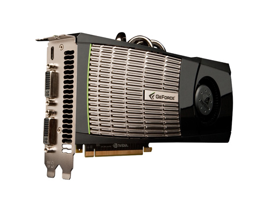
Today NVIDIA is launching two cards: the GeForce GTX 480, and the GeForce GTX 470. Both of them are based on GF100, the first and largest member of the Fermi family. Right off the bat, we can tell you that neither card is a complete GF100 chip. We know from NVIDIA's earlier announcements that a complete GF100 is a 512 SP/core part organized in a 4x16x32 fashion, but these first parts will not have all of GF100's functional units activated. Instead we'll be getting a 480 core part for the GTX 480, and a 448 core part for the GTX 470. Ultimately we will not be seeing the full power of GF100 right away, but you can be sure that somewhere down the line we'll see a GTX 485 or GTX 490 with all of GF100's functional units enabled.
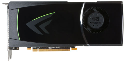
 NVIDIA's GeForce GTX 480
What we're starting out with today at the high-end is the GTX 480, a card based on a GF100 with 1 of the 16 SMs disabled that will sell for $499, making it the primary competitor for the Radeon 5870. The disabled SM has no affect on the ROPs which are part of a separate functional block, but it does cut down on the shading, texturing, and tessellation capabilities of the card compared to where a full GF100 card would be. This gives the GTX 480 the full 48 ROPs and 768KB of L2 cache of GF100, along with 60 texture units, 15 PolyMorph engines, and 480 cores. Although the architectural overhaul means we can't compare the GTX 480 to the GTX 285 quite as easily as we could the Radeon 5000 series to the Radeon 4000 series, the GTX 480 is still in some ways a doubled-up GTX 285 from a shader standpoint.
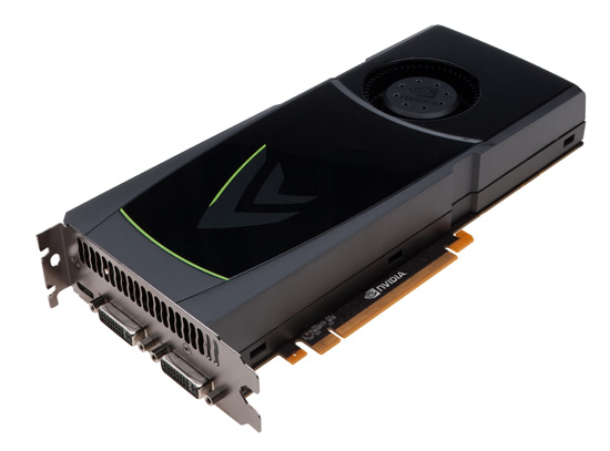
The GTX 470 on the other hand is a further cut-down GF100-based product that will sell for $349. As we stated earlier it has only 448 cores, a product of NVIDIA disabling 2 of the 16 SMs. Along with disabling the SMs, NVIDIA also disabled 1 of the 6 ROP clusters, which disables 6 ROPs, 128KB of L2 cache, and 2 of the 32bit memory channels. This leaves us with 448 cores running alongside 40 ROPs, 640KB of L2 cache, all on a 320bit GDDR5 memory bus.
 NVIDIA's GeForce GTX 470
As is usually the case for a harvested part, GTX 470 takes a clockspeed hit compared to GTX 480. The core clock falls 13% to 607MHz, and the shader clock falls the same distance to 1215MHz. The memory clock on the other hand only drops by 10% to 837MHz (3348MHz effective). Overall this gives the GTX 470 around 80% of the shading, texturing, and tessellation capabilities of the GTX 480 and 72% of the ROP capability and memory bandwidth.
One thing that caught our eye with all of this was that NVIDIA's memory clocks are lower than we had been initially expecting. GDDR5 is readily available up to 5GHz while NVIDIA doesn't go any higher than 3.7GHz; in fact between the smaller memory bus than the GTX 285 and the lower than expected memory clocks, the GTX 400 series doesn't have all that much more bandwidth than the GTX 285 did. As it stands the GTX 480 only has 11% more memory bandwidth than the GTX 285, while the GTX 470 has 15% less than the GTX 285.
Given the 384-bit bus, we initially assumed NVIDIA was running in to even greater memory bus issues than AMD ran in to for the 5000 series, but as it turns out that's not the case. When we asked NVIDIA about working with GDDR5, they told us that their biggest limitation wasn't the bus like AMD but rather deficiencies in their own I/O controller, which in turn caused them to miss their targeted memory speeds. Unlike AMD who has been using GDDR5 for nearly 2 years, NVIDIA is still relatively new at using GDDR5 (their first product was the GT 240 late last year), so we can't say we're completely surprised here. If nothing else, this gives NVIDIA ample room to grow in the future if they can get a 384-bit memory bus up to the same speeds as AMD has gotten their 256-bit bus.
This leaves us with the other elephant in the room: yield on GF100. NVIDIA hasn't commented specifically on the yields coming out of TSMC but we know even 6 months later that AMD still isn't satisfied with things, so that should offer some guidance on the situation given NVIDIA's larger die. As it stands NVIDIA chose to launch their highest end GF100 part with only 15 of 16 SMs in order to reach the “broadest availability”, which is a clear sign that NVIDIA isn't getting enough full-yielding and high-clocking dies at this time to offer a proper unharvested part.
The power/heat situation also bears mentioning, since it often goes hand-in-hand with yield issues. With a 500mm2+ die on the 40nm process, it should come as no surprise that both the GTX 480 and GTX 470 are hot cards. NVIDIA has to pay the piper for having such a large die, and this is one of the places where they do so. The TDP for the GTX 480 is 250W while it's 215W for the GTX 470; meanwhile the cards idle at 47W and 33W respectively. NVIDIA's large die strategy usually leads to them having power-hungry parts, but from a historical perspective the GTX 480 is the hungriest yet for a single-GPU card; even the GTX280 wasn't quite as high. We'll get in to this more when we take a look at measured power consumption.
Meet the GTX 480 and GTX 470, Cont
Moving beyond the GF100 GPU itself, we have the boards. With NVIDIA once more forgoing a power-of-two sized memory bus on their leading part, the number of memory chips and the total memory size of the GTX 400 series is once again an odd amount. On the GTX 480 there are 12 128MB GDDR5 memory chips for a total of 1536MB of VRAM, while the GTX 470 has 10 chips for a total of 1280MB. This marks the first big expansion in memory capacity we've seen out of NVIDIA in quite some time; after introducing the 8800GTX in 2006 with 768MB of RAM, we haven't seen them do anything besides bump up 256-bit/512-bit memory bus parts to 1GB over the years. And with 256MB GDDR5 due in volume later this year, we wouldn't be surprised to see NVIDIA push a 3GB part before the year is out.
Meanwhile in a stark difference from the GTX 200 series, the GTX 400 series does not share a common design and cooler. This leads to the GTX 480 and GTX 470 being remarkably different cards. The GTX 470 is essentially a slight variation on the GTX 200 series design, utilizing a similar fully shrouded design as those cards. Meanwhile the GTX 480 is positively alien coming from the GTX 200 series in two distinct ways. The first is the 4 heatpipes from the top of the card (with a 5th one saying within the card), and the second is the fully exposed heatsink grill on the front of the card. That's exactly what it looks like folks – that's the top of the heatsink on the GTX 480. At this point it's mostly an intellectual curiosity (we have no idea whether it makes the GTX 480's cooler all that better) but we did learn the hard way that it's not just cosmetic, it can get very hot.
One new thing that both cards do share in common is that the shroud is no longer a single large device; on the GTX 480 and GTX 470 the top of the shroud can be snapped on and off, allowing easy access to the heatsink and fan assemblies. We can't imagine that most users will ever want to remove the top of the shroud, but this is one of the cooler design elements we've seen in a video card in recent years. It'll be interesting to see if this proves to be beneficial for aftermarket coolers, as this should make installation/uninstallation much more expedient.
One other common element between the cards is that they have a cut-out PCB for pulling in air both from the front side and the back side of the card. We've seen this before on the GTX 295, but this is the first time we've seen this design element on a single-GPU card.
For those of you working with cramped cases, you should find these cards to be a pleasant surprise. The GTX 470 is 9.5", making it the same length as the Radeon 5850 (or nearly 1" shorter than the GTX 200 series). On the other hand the GTX 480 measures 10.5", which is ever so slightly longer than the GTX 200 series which we measure at 10.45". We're also happy to report that NVIDIA put the PCIe power plugs on the top of both cards, rather than on the rear of the card as AMD did on the Radeon 5850. Practically speaking, both of these cards should fit in to a wider array cases than AMD's respective cards.
Even though these cards will fit in to smaller cases though, airflow will be paramount due to the high TDP of these cards. NVIDIA's own reviewers guide even goes so far as to recommend spacing your cards out as far as possible for SLI use. This actually isn't a bad idea no matter what cards are involved since it ensure neither card is restricted by the other, however given that not every board with a 3rd PCIe x16 slot offers full bandwidth to that slot, it's not a practical suggestion for all cases. If you can't separate your cards, you're going to want great airflow instead, such as putting a fan directly behind the cards.
Up next is the port layout of the GTX 400 series. Unlike AMD, NVIDIA's TDP is too high here to go with a half-slot vent here, so NVIDIA is limited to what ports they can fit on a single full slot. In this case their reference design is a pair of DVI ports and a mini-HDMI port (this being the first cards with that port in our labs). Bear in mind that GF100 doesn't have the ability to drive 3 displays with a single card, so while there are 3 DVI-type outputs here, you can only have two at once.
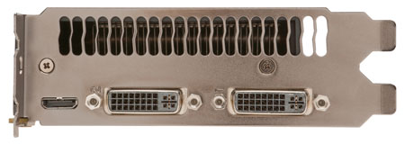
After having seen DisplayPort on virtually every AMD card in our labs, we were caught a bit off guard by the fact that NVIDIA didn't do the same and go with something like a mini-DisplayPort here for a 2x DVI + 1x mini-DP configuration like we've seen on the Radeon 5970. NVIDIA tells us that while they could do such a thing, their market research has shown that even their high-end customers are more likely to purchase a monitor with HDMI than with DP, hence the decision to go with mini-HDMI. This is somewhat academic since DVI can easily be converted to HDMI, but this allows NVIDIA's partners to skip the dongles and makes it easier to do audio pass-through for monitors with built-in speakers.
Speaking of audio, let's quickly discuss the audio/video capabilities of the GTX 400 series. GF100 has the same audio/video capabilities as the 40nm GT 200 series launched late last year, so this means NVIDIA's VP4 for video decoding (H.264/MPEG-2/VC-1/MPEG-4 ASP) and internal passthrough for audio. Unfortunately the latter means that the GTX 400 series (and other first-generation Fermi derivatives) won't be able to match AMD's Radeon 5000 series in audio capabilities – NVIDIA can do compressed lossy audio(DD/DTS) and 8 channel uncompressed LPCM, but not lossless compressed audio formats such as DTS-HD and Dolby TrueHD. This leaves the HTPC crown safely in AMD's hands for now.
Finally we bad news: availability. This is a paper launch; while NVIDIA is launching today, the cards won't be available for another two and a half weeks at a minimum. NVIDIA tells us that the cards are expected to reach retailers on the week of April 12th, which hopefully means the start of that week and not the end of it. In either case we have to chastise NVIDIA for this; they've managed to have hard launches in the past without an issue, so we know they can do better than this. This is a very bad habit to get in to.
Once these cards do go on sale, NVIDIA is telling us that the actual launch supply is going to be in the tens-of-thousands of units. How many tens-of-thousands? We have no idea. For the sake of comparison AMD had around 30,000 units for the 5800 series launch, and those were snapped up in an instant. We don't think NVIDIA's cards will sell quite as quickly due to the pricing and the fact that there's viable competition for this launch, but it's possible to have tens-of-thousands of units and still sell out in a heartbeat. This is something we'll be watching intently in a couple of weeks.
The availability situation also has us concerned about card prices. NVIDIA is already starting off behind AMD in terms of pricing flexibility; 500mm3+ dies and 1.5GB of RAM does not come cheap. If NVIDIA does manage to sell the GTX 400 series as fast as they can send cards out then there's a good chance there will be a price hike. AMD is in no rush to lower prices and NVIDIA's higher costs mean that if they can get a higher price they should go for it. With everything we've seen from NVIDIA and AMD, we're not ready to rule out any kind of price hike, or to count on any kind of price war.
The GF100 Recap
NVIDIA first unveiled its GF100 (then called Fermi) architecture last September. If you've read our Fermi and GF100 architecture articles, you can skip this part. Otherwise, here's a quick refresher on how this clock ticks.
First, let’s refresh the basics. NVIDIA’s GeForce GTX 480 and 470 are based on the GF100 chip, the gaming version of what was originally introduced last September as Fermi. GF100 goes into GeForces and Fermi goes into Tesla cards. But fundamentally the two chips are the same.
At a high level, GF100 just looks like a bigger GT200, however a lot has changed. It starts at the front end. Prior to GF100 NVIDIA had a large unified front end that handled all thread scheduling for the chip, setup, rasterization and z-culling. Here’s the diagram we made for GT200 showing that:
NVIDIA's GT200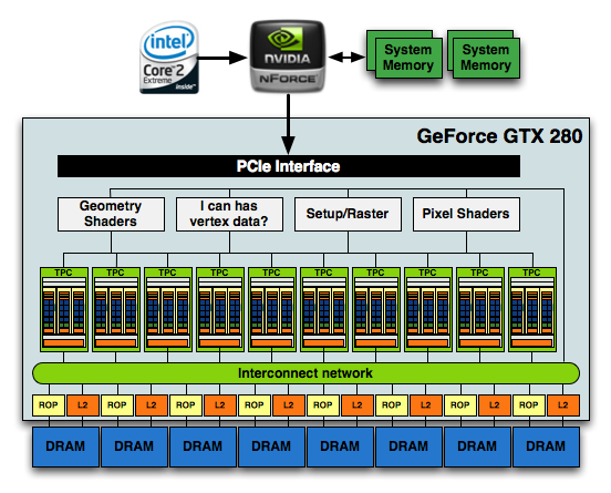
The grey boxes up top were shared by all of the compute clusters in the chip below. In GF100, the majority of that unified front end is chopped up and moved further down the pipeline. With the exception of the thread scheduling engine, everything else decreases in size, increases in quantity and moves down closer to the execution hardware. It makes sense. The larger these chips get, the harder it is to have big unified blocks feeding everything.
In the old days NVIDIA took a bunch of cores, gave them a cache, some shared memory and a couple of special function units and called the whole construct a Streaming Multiprocessor (SM). The GT200 took three of these SMs, added texture units and an L1 texture cache (as well as some scheduling hardware) and called it a Texture/Processor Cluster. The old GeForce GTX 280 had 10 of these TPCs and that’s what made up the execution engine of the GPU.
NVIDIA's GF100
Click to Enlarge
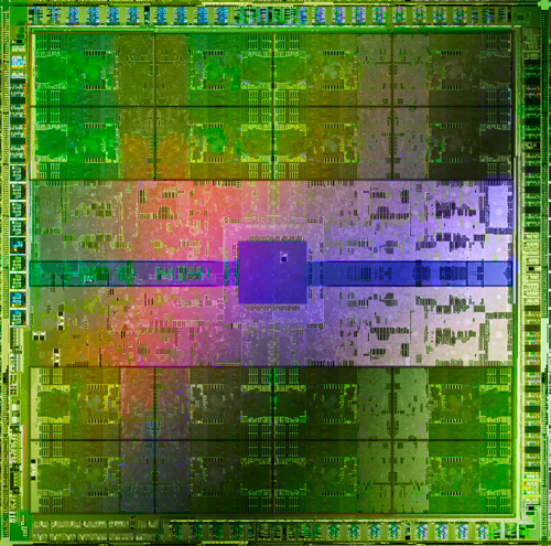
With GF100, the TPC is gone. It’s now a Graphics Processing Cluster (GPC) and is made up of much larger SMs. Each SM now has 32 cores and there are four SMs per GPC. Each GPC gets its own raster engine, instead of the entire chip sharing a larger front end. There are four GPCs on a GF100 (however no GF100 shipping today has all SMs enabled in order to improve yield).

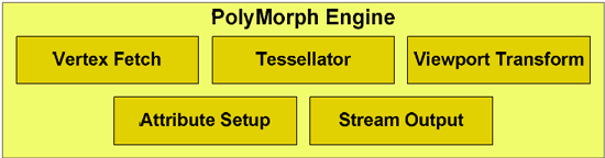
Each SM also has what NVIDIA is calling a PolyMorph engine. This engine is responsible for all geometry execution and hardware tessellation, something NVIDIA expects to be well used in DX11 and future games. NV30 (GeForce FX 5800) and GT200 (GeForce GTX 280), the geometry performance of NVIDIA’s hardware only increases roughly 3x in performance. Meanwhile the shader performance of their cards increased by over 150x. Compared just to GT200, GF100 has 8x the geometry performance of GT200, and NVIDIA tells us this is something they have measured in their labs. This is where NVIDIA hopes to have the advantage over AMD, assuming game developers do scale up geometry and tessellation use as much as NVIDIA is counting on.
NVIDIA also clocks the chip much differently than before. In the GT200 days we had a core clock, a shader clock and a memory clock. The core clock is almost completely out of the picture now. Only the ROPs and L2 cache operate on a separate clock domain. Everything else runs at a derivative of the shader clock. The execution hardware runs at the full shader clock speed, while the texture units, PolyMorph and Raster engines all run at 1/2 shader clock speed.
Cores and MemoryWhile we’re looking at GF100 today through gaming colored glasses, NVIDIA is also trying to build an army of GPU compute cards. In serving that master, the GF100’s architecture also differs tremendously from its predecessors.
All of the processing done at the core level is now to IEEE spec. That’s IEEE-754 2008 for floating point math (same as RV870/5870) and full 32-bit for integers. In the past 32-bit integer multiplies had to be emulated, the hardware could only do 24-bit integer muls. That silliness is now gone. Fused Multiply Add is also included. The goal was to avoid doing any cheesy tricks to implement math. Everything should be industry standards compliant and give you the results that you’d expect. Double precision floating point (FP64) performance is improved tremendously. Peak 64-bit FP execution rate is now 1/2 of 32-bit FP, it used to be 1/8 (AMD's is 1/5).

GT200 SM
In addition to the cores, each SM has a Special Function Unit (SFU) used for transcendental math and interpolation. In GT200 this SFU had two pipelines, in GF100 it has four. While NVIDIA increased general math horsepower by 4x per SM, SFU resources only doubled. The infamous missing MUL has been pulled out of the SFU, we shouldn’t have to quote peak single and dual-issue arithmetic rates any longer for NVIDIA GPUs.

GF100 SM
NVIDIA’s GT200 had a 16KB shared memory in each SM. This didn’t function as a cache, it was software managed memory. GF100 increases the size to 64KB but it can operate as a real L1 cache now. In order to maintain compatibility with CUDA applications written for G80/GT200 the 64KB can be configured as 16/48 or 48/16 shared memory/L1 cache. GT200 did have a 12KB L1 texture cache but that was mostly useless for CUDA applications. That cache still remains intact for graphics operations. All four GPCs share a large 768KB L2 cache.

Each SM has four texture units, each capable of 1 texture address and 4 texture sample ops. We have more texture sampling units but fewer texture addressing units in GF100 vs. GT200. All texture hardware runs at 1/2 shader clock and not core clock.
| NVIDIA Architecture Comparison | G80 | G92 | GT200 | GF100 | GF100 Full* |
| Streaming Processors per TPC/GPC | 16 | 16 | 24 | 128 | 128 |
| Texture Address Units per TPC/GPC | 4 | 8 | 8 | 16 | 16 |
| Texture Filtering Units per TPC/GPC | 8 | 8 | 8 | 64 | 64 |
| Total SPs | 128 | 128 | 240 | 480 | 512 |
| Total Texture Address Units | 32 | 64 | 80 | 60 | 64 |
| Total Texture Filtering Units | 64 | 64 | 80 | 240 | 256 |
Last but not least, this brings us to the ROPs. The ROPs have been reorganized, there are now 48 of them in 6 parttions of 8, and a 64bit memory channel serving each partition. The ROPs now share the L2 cache with the rest of GF100, while under GT200 they had their own L2 cache. Each ROP can do 1 regular 32bit pixel per clock, 1 FP16 pixel over 2 clocks, or 1 FP32 pixel over 4 clocks, giving the GF100 the ability to retire 48 regular pixels per clock. The ROPs are clocked together with the L2 cache.
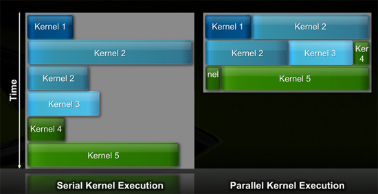
Threads and SchedulingWhile NVIDIA’s G80 didn’t start out as a compute chip, GF100/Fermi were clearly built with general purpose compute in mind from the start. Previous architectures required that all SMs in the chip worked on the same kernel (function/program/loop) at the same time. If the kernel wasn’t wide enough to occupy all execution hardware, that hardware went idle, and efficiency dropped as a result. Remember these chips are only powerful when they’re operating near 100% utilization.
In this generation the scheduler can execute threads from multiple kernels in parallel, which allowed NVIDIA to scale the number of cores in the chip without decreasing efficiency.
GT200 (left) vs. GF100 (right)
With a more compute leaning focus, GF100 also improves switch time between GPU and CUDA mode by a factor of 10x. It’s now fast enough to switch back and forth between modes multiple times within a single frame, which should allow for more elaborate GPU accelerated physics.
NVIDIA’s GT200 was a thread monster. The chip supported over 30,000 threads in flight. With GF100, NVIDIA scaled that number down to roughly 24K as it found that the chips weren’t thread bound but rather memory bound. In order to accommodate the larger shared memory per SM, max thread count went down.
| GF100 | GT200 | G80 | |
| Max Threads in Flight | 24576 | 30720 | 12288 |
NVIDIA groups 32 threads into a unit called a warp (taken from the looming term warp, referring to a group of parallel threads). In GT200 and G80, half of a warp was issued to an SM every clock cycle. In other words, it takes two clocks to issue a full 32 threads to a single SM.
In previous architectures, the SM dispatch logic was closely coupled to the execution hardware. If you sent threads to the SFU, the entire SM couldn't issue new instructions until those instructions were done executing. If the only execution units in use were in your SFUs, the vast majority of your SM in GT200/G80 went unused. That's terrible for efficiency.
Fermi fixes this. There are two independent dispatch units at the front end of each SM in Fermi. These units are completely decoupled from the rest of the SM. Each dispatch unit can select and issue half of a warp every clock cycle. The threads can be from different warps in order to optimize the chance of finding independent operations.
There's a full crossbar between the dispatch units and the execution hardware in the SM. Each unit can dispatch threads to any group of units within the SM (with some limitations).
The inflexibility of NVIDIA's threading architecture is that every thread in the warp must be executing the same instruction at the same time. If they are, then you get full utilization of your resources. If they aren't, then some units go idle.
A single SM can execute:
| GF100 | FP32 | FP64 | INT | SFU | LD/ST |
| Ops per clock | 32 | 16 | 32 | 4 | 16 |
If you're executing FP64 instructions the entire SM can only run at 16 ops per clock. You can't dual issue FP64 and SFU operations.
The good news is that the SFU doesn't tie up the entire SM anymore. One dispatch unit can send 16 threads to the array of cores, while another can send 16 threads to the SFU. After two clocks, the dispatchers are free to send another pair of half-warps out again. As I mentioned before, in GT200/G80 the entire SM was tied up for a full 8 cycles after an SFU issue.
The flexibility is nice, or rather, the inflexibility of GT200/G80 was horrible for efficiency and Fermi fixes that.
Odds & Ends: ECC & NVIDIA Surround Missing
One of the things we have been discussing with NVIDIA for this launch is ECC. As we just went over in our GF100 Recap, Fermi offers ECC support for its register file, L1 cache, L2 cache, and RAM. The latter is the most interesting, as under normal circumstances implementing ECC requires a wider bus and additional memory chips. The GTX 400 series will not be using ECC, but we went ahead and asked NVIDIA how ECC will work on Fermi products anyhow.
To put things in perspective, for PC DIMMs an ECC DIMM will be 9 chips per channel (9 bits per byte) hooked up to a 72bit bus instead of 8 chips on a 64bit bus. However NVIDIA doesn’t have the ability or the desire to add even more RAM channels to their products, not to mention 8 doesn’t divide cleanly in to 10/12 memory channels. So how do they implement ECC?
The short answer is that when NVIDIA wants to enable ECC they can just allocate RAM for the storage of ECC data. When ECC is enabled the available RAM will be reduced by 1/8th (to account for the 9th ECC bit) and then ECC data will be distributed among the RAM using that reserved space. This allows NVIDIA to implement ECC without the need for additional memory channels, at the cost of some RAM and some performance.
On the technical side, despite this difference in implementation NVIDIA tells us that they’re still using standard Single Error Correction / Double Error Detection (SECDED) algorithms, so data reliability is the same as in a traditional implementation. Furthermore NVIDIA tells us that the performance hit isn’t a straight-up 12.5% reduction in effective memory bandwidth, rather they have ways to minimize the performance hit. This is their “secret sauce” as they call it, and it’s something that they don’t intend to discuss at in detail at this time.
Shifting gears to the consumer side, back in January NVIDIA was showing off their Eyefinity-like solutions 3DVision Surround and NVIDIA Surround on the CES showfloor. At the time we were told that the feature would launch with what is now the GTX 400 series, but as with everything else related to Fermi, it’s late.
Neither 3DVision Surround nor NVIDIA surround are available in the drivers sampled to us for this review. NVIDIA tells us that these features will be available in their release 256 drivers due in April. There hasn’t been any guidance on when in April these drivers will be released, so at this point it’s anyone’s guess whether they’ll arrive in time for the GTX 400 series retail launch.
Tessellation & PhysX
Well kick off our in-depth look at the performance of the GTX400 series with Tessellation and PhysX. These are two of the biggest features that NVIDIA is pushing with the GTX400 series, with tessellation in particular being the major beneficiary of NVIDIAs PolyMorph Engine strategy.
As we covered in our GF100 Recap, NVIDIA seeks to separate themselves from AMD in spite of the rigid feature set imposed by DirectX 11. Tessellation is one of the ways they intend to do that, as the DirectX 11 standard leaves them plenty of freedom with respect to tessellation performance. To accomplish this goal, NVIDIA needs significantly better tessellation performance, which has lead to them having 14/15/16 tesselators through having that many PolyMorph Engines. With enough tessellation performance NVIDIA can create an obvious image quality improvement compared to AMD, all the while requiring very little on the part of developers to take advantage of this.
All things considered, NVIDIAs claim of having superior tessellation performance is one of the easiest claims to buy, but all the same weve gone ahead and attempted to confirm it.
Our first tessellation test is the newly released Unigine Heaven 2.0 benchmark, which was released a few days ago. 2.0 added support for multiple levels of tessellation (with 1.0 having earned a reputation of using extreme levels of tessellation), which allows us to look at tessellation performance by varying tessellation levels. If the GTX 480s tessellation capabilities are several times faster than the Radeon 5870s as NVIDIA claims, then it should better handle the increased tessellation levels.
Since Heaven is a largely a synthetic benchmark at the moment (the DX11 engine isnt currently used in any games) well be focusing on the relative performance of cards to themselves in keeping with our editorial policy of avoiding synthetic GPU tests when possible.
Heaven: Moderate & Extreme Tessellation
Heaven has 4 tessellation levels: off, moderate, normal, extreme. For our test were using the moderate and extreme modes, comparing the performance of extreme as a percentage of moderate performance.
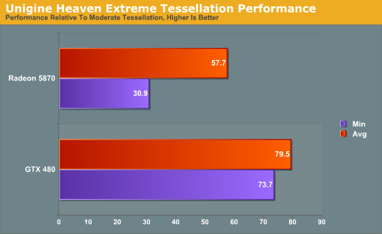
Starting with averages, the GTX 480 keeps 79% of its performance moving from moderate to extreme. On the Radeon 5870 however, the performance drop-off is much more severe, losing 42% of its performance to bring it down to 58%.
The minimum framerates are even more telling. The GTX 480 minimum framerates drop by 26% when switching to extreme tessellation. The Radeon 5870 is much worse off here, bringing in minimum framerates 69% lower when using extreme tessellation. From these numbers its readily apparent that the GTX 480 is much more capable of dealing with very high tessellation levels than the Radeon 5870 is.
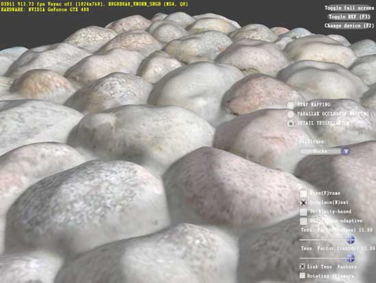
Our second tessellation test is similar in nature, this time taken from one of Microsofts DX11 sample programs: Detail Tessellation. Detail Tessellation is a simple scene where tessellation plus displacement mapping is used to turn a flat rock texture in to a simulated field of rocks by using tessellation to create the geometry. Here we measure the average framerate at different tessellation factors (7 and 11) and compare the framerate at the higher tessellation factor to the lower tessellation factor.
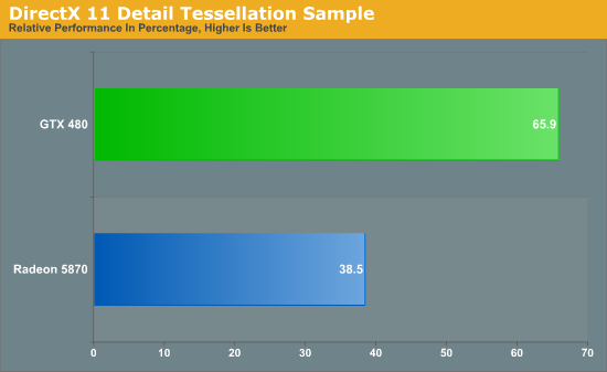
Looking at just the averages (the framerate is rather solid) we see that the GTX 480 retains 65% of its performance moving from factor 7 to factor 11. The Radeon 5870 on the other hand only retains 38% of its performance. Just as what we saw in Unigine, the GTX 480 takes a much lighter performance hit from higher tessellation factors than the Radeon 5870 does, driving home the point that the GTX 480 has a much more powerful tessellator.
With the results of these tests, theres no reason to doubt NVIDIAs claims about GF100s tessellation abilities. All the data we have points GF100/GTX 480 being much more powerful than the Radeon 5000 series when it comes to tessellation.
But with that said, NVIDIA having a more powerful tessellator doesnt mean much on its own. Tessellation is wholly dependent on game developers to make use of it and to empower users to adjust the tessellation levels. Currently every DX11 game using tessellation uses a fixed amount of it, so NVIDIAs extra tessellation abilities are going unused. This doesnt mean that tessellation will always be used like this, but it means things have to change, and counting on change is a risky thing.
NVIDIAs superior tessellation abilities will require that developers offer a variable degree of tessellation in order to fully utilize their tessellation hardware, and that means NVIDIA needs to convince developers to do the extra work to implement this. At this point theres no way for us to tell how things will go: NVIDIAs superior tessellation abilities could be the next big thing that seperates them from AMD like theyre shooting for, or it could be the next DirectX 10.1 by being held back by weaker hardware. Without some better sense of direction on the future use of tessellation, we cant make any recommendations based on NVIDIAs greater tessellation performance.
Moving on we have PhysX, NVIDIAs in-house physics simulation middleware. After picking up PhysX and its developer AGEIA in 2008, NVIDIA re-implemented PhysX hardware acceleration as a CUDA application, allowing their GPUs to physics simulations in hardware. NVIDIA has been pushing it on developers and consumers alike with limited success, and PhysX only finally had a breakthrough title last year with the critically acclaimed Batman: Arkham Asylum.
With Fermis greatly enhanced compute abilities, NVIDIA is now pushing the idea that PhysX performance will be much better on Fermi cards, allowing developers to use additional and more complex physics actions than ever before. In particular, with the ability to use concurrent kernels and the ability to do fast context switching, PhysX should have a reduced degree of overhead on Fermi hardware than it did on GT200/G80 hardware.
To put this idea to the test, we will be using the Batman: Arkham Asylum benchmark to measure PhysX performance. If PhysX has less overhead on Fermi hardware then the framerate hit on the GTX 480 from enabling PhysX effects should be lower than the framerate hit on the GTX 285. For this test we are running at 2560x1600, comparing performance between PhysX being disabled and when its set on High.
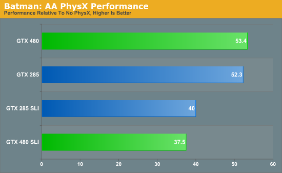
If PhysX has less overhead on Fermi hardware, Batman is not the game to show it. On both the GTX 480 and the GTX 285, the performance hit on a percentage basis for enabling PhysX is roughly 47%. The GTX 480 may be faster overall, but it takes the same heavy performance hit for enabling PhysX. The SLI cards fare even worse here: the performance hit for enabling PhysX is 60% on both the GTX 480 SLI and the GTX 285 SLI.
PhysX unquestionably has the same amount of overhead on the GTX 480 as it does the GTX 285. If PhysX is going to take up less overhead, then from what we can gather it either will be a benefit limited to PhysX 3, or will require future PhysX 2.x updates that have yet to be delivered.
Or second PhysX test is a more generalized look at PhysX performance. Here were using NVIDIAs Raging Rapids tech demo to measure PhysX performance. Raging Rapids is a water simulation demonstration that uses PhysX to simulate waves, waterfalls, and more. Here we are measuring the framerate in the demos benchmark mode.
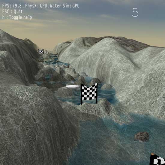
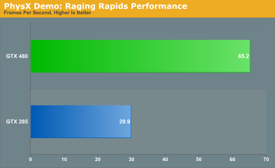
Overall the Raging Rapids benchmark gives us mixed results. Out of all of the benchmarks we have run on the GTX 480, this is one of the larger performance jumps over the GTX 285. On the other hand, once we compensate for the GTX 480s additional shaders, we end up with a result only around 10% faster than a strict doubling in performance. This is a sign of good scaling, but it isnt a sign that the GTX 480 is significantly faster than the GTX 285 due to more efficient use of compute resources. Just having all of this extra compute power is certainly going to make a difference overall, but on an architectural level the GTX 480 doesnt look to be significantly faster at PhysX than the GTX 285 on a per-clock/per-shader basis.
Compute
Continuing at our look at compute performance, we’re moving on to more generalized compute tasks. GPGPU has long been heralded as the next big thing for GPUs, as in the right hands at the right task they will be much faster than a CPU would be. Fermi in turn is a serious bet on GPGPU/HPC use of the GPU, as a number of architectural tweaks went in to Fermi to get the most out of it as a compute platform. The GTX 480 in turn may be targeted as a gaming product, but it has the capability to be a GPGPU powerhouse when given the right task.
The downside to GPGPU use however is that a great deal of GPGPU applications are specialized number-crunching programs for business use. The consumer side of GPGPU continues to be underrepresented, both due to a lack of obvious, high-profile tasks that would be well-suited for GPGPU use, and due to fragmentation in the marketplace due to competing APIs. OpenCL and DirectCompute will slowly solve the API issue, but there is still the matter of getting consumer orientated GPGPU applications out in the first place.
With the introduction of OpenCL last year, we were hoping by the time Fermi was launched that we would see some suitable consumer applications that would help us evaluate the compute capabilities of both AMD and NVIDIA’s cards. That has yet to come to pass, so at this point we’re basically left with synthetic benchmarks for doing cross-GPU comparisons. With that in mind we’ve run a couple of different things, but the results should be taken with a grain of salt as they don’t represent any single truth about compute performance on NVIDIA or AMD’s cards.
Out of our two OpenCL benchmarks, we’ll start with an OpenCL implementation of an N-Queens solver from PCChen of Beyond3D. This benchmark uses OpenCL to find the number of solutions for the N-Queens problem for a board of a given size, with a time measured in seconds. For this test we use a 17x17 board, and measure the time it takes to generate all of the solutions.
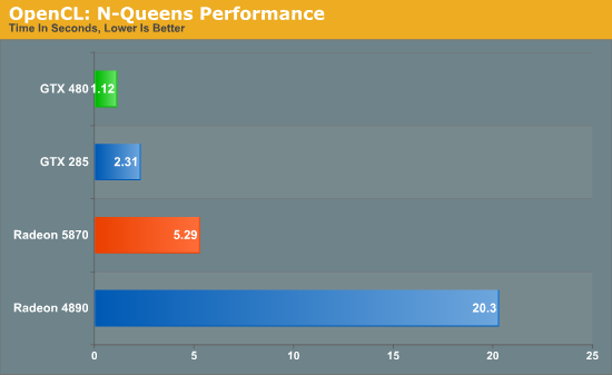
This benchmark offers a distinct advantage to NVIDIA GPUs, with the GTX cards not only beating their AMD counterparts, but the GTX 285 also beating the Radeon 5870. Due to the significant underlying differences of AMD and NVIDIA’s shaders, even with a common API like OpenCL the nature of the algorithm still plays a big part in the performance of the resulting code, so that may be what we’re seeing here. In any case, the GTX 480 is the fastest of the GPUs by far, beating out the GTX 285 by over half the time, and coming in nearly 5 times faster than the Radeon 5870.
Our second OpenCL benchmark is a post-processing benchmark from the GPU Caps Viewer utility. Here a torus is drawn using OpenGL, and then an OpenCL shader is used to apply post-processing to the image. Here we measure the framerate of the process.
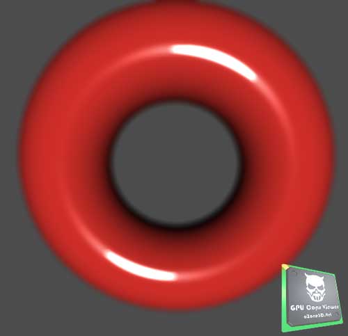
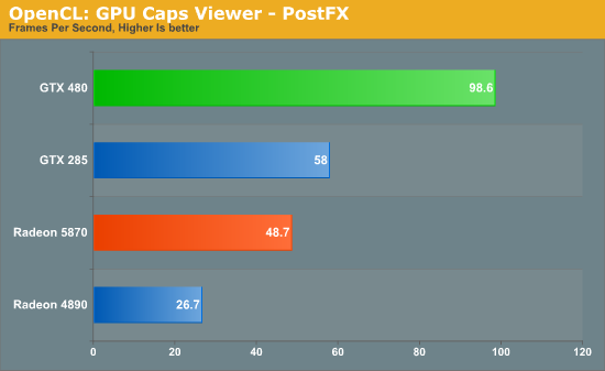
Once again the NVIDIA cards do exceptionally well here. The GTX 480 is the clear winner, while even the GTX 285 beats out both Radeon cards. This could once again be the nature of the algorithm, or it could be that the GeForce cards really are that much better at OpenCL processing. These results are going to be worth keeping in mind as real OpenCL applications eventually start arriving.
Moving on from cross-GPU benchmarks, we turn our attention to CUDA benchmarks. Better established than OpenCL, CUDA has several real GPGPU applications, with the limit being that we can’t bring the Radeons in to the fold here. So we can see how much faster the GTX 480 is over the GTX 285, but not how this compares to AMD’s cards.
We’ll start with Badaboom, Elemental Technologies’ GPU-accelerated video encoder for CUDA. Here we are encoding a 2 minute 1080i clip and measuring the framerate of the encoding process.
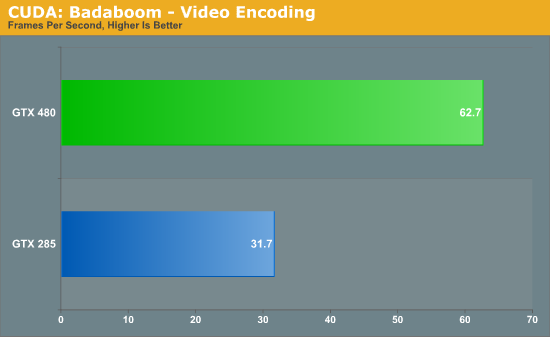
The performance difference with Badaboom is rather straightforward. We have twice the shaders running at similar clockspeeds, and as a result we get twice the performance. The GTX 480 encodes our test clip in a little over half the time it took the GTX 280.
Up next is a special benchmark version of Folding@Home that has added Fermi compatibility. Folding@Home is a Standford research project that simulates protein folding in order to better understand how misfolded proteins lead to diseases. It has been a poster child of GPGPU use, having been made available on GPUs as early as 2006 as a Close-To-Metal application for AMD’s X1K series of GPUs. Here we’re measuring the time it takes to fully process a sample work unit so that we can project how many nodes (units of work) a GPU could complete per day when running Folding@Home.
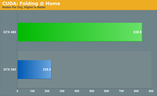
Folding@Home is the first benchmark we’ve seen that really showcases the compute potential for Fermi. Unlike everything else which has the GTX 480 running twice as fast as the GTX 285, the GTX 480 is a fewtimes faster than the GTX 285 when it comes to folding. Here a GTX 480 would get roughly 3.5x as much work done per day as a GTX 285. And while this is admittedly more of a business/science application than it is a home user application (even if it’s home users running it), it gives us a glance at what Fermi is capable when it comes to compuete.
Last, but not least for our look at compute, we have another tech demo from NVIDIA. This one is called Design Garage, and it’s a ray tracing tech demo that we first saw at CES. Ray tracing has come in to popularity as of late thanks in large part to Intel, who has been pushing the concept both as part of their CPU showcases and as part of their Larrabee project.
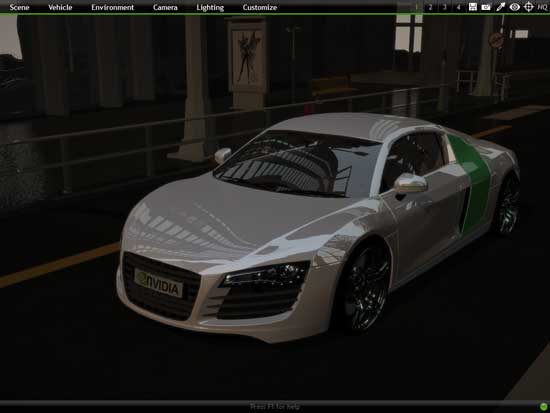
In turn, Design Garage is a GPU-powered ray tracing demo, which uses ray tracing to draw and illuminate a variety of cars. If you’ve never seen ray tracing before it looks quite good, but it’s also quite resource intensive. Even with a GTX 480, with the high quality rendering mode we only get a couple of frames per second.
On a competitive note, it’s interesting to see NVIDIA try to go after ray tracing since that has been Intel’s thing. Certainly they don’t want to let Intel run around unchecked in case ray tracing and Larrabee do take off, but at the same time it’s rasterization and not ray tracing that is Intel’s weak spot. At this point in time it wouldn’t necessarily be a good thing for NVIDIA if ray tracing suddenly took off.
Much like the Folding@Home demo, this is one of the best compute demos for Fermi. Compared to our GTX 285, the GTX 480 is eight times faster at the task. A lot of this comes down to Fermi’s redesigned cache, as ray tracing as a high rate of cache hits which help to avoid hitting up the GPU’s main memory any more than necessary. Programs that benefit from Fermi’s optimizations to cache, concurrency, and fast task switching apparently stand to gain the most in the move from GT200 to Fermi.
Image Quality & AA
When it comes to image quality, the big news from NVIDIA for Fermi is what NVIDIA has done in terms of anti-aliasing of fake geometry such as billboards. For dealing with suck fake geometry, Fermi has several new tricks.
The first is the ability to use coverage samples from CSAA to do additional sampling of billboards that allow Alpha To Coverage sampling to fake anti-alias the fake geometry. With the additional samples afforded by CSAA in this mode, the Fermi can generate additional transparency levels that allow the billboards to better blend in as properly anti-aliased geometry would.
The second change is a new CSAA mode: 32x. 32x is designed to go hand-in-hand with the CSAA Alpha To Coverage changes by generating an additional 8 coverage samples over 16xQ mode for a total of 32 samples and giving a total of 63 possible levels of transparency on fake geometry using Alpha To Coverage.
In practice these first two changes haven’t had the effect we were hoping for. Coming from CES we thought this would greatly improve NVIDIA’s ability to anti-alias fake geometry using cheap multisampling techniques, but apparently Age of Conan is really the only game that greatly benefits from this. The ultimate solution is for more developers of DX10+ applications to enable Alpha To Coverage so that anyone’s MSAA hardware can anti-alias their fake geometry, but we’re not there yet.
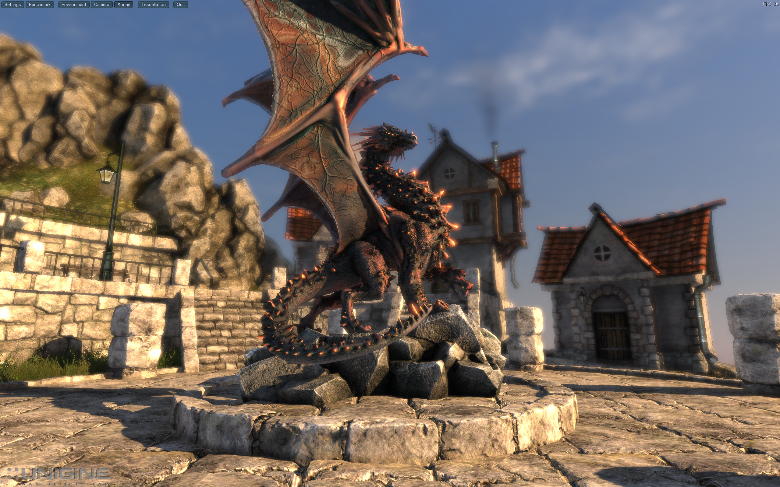
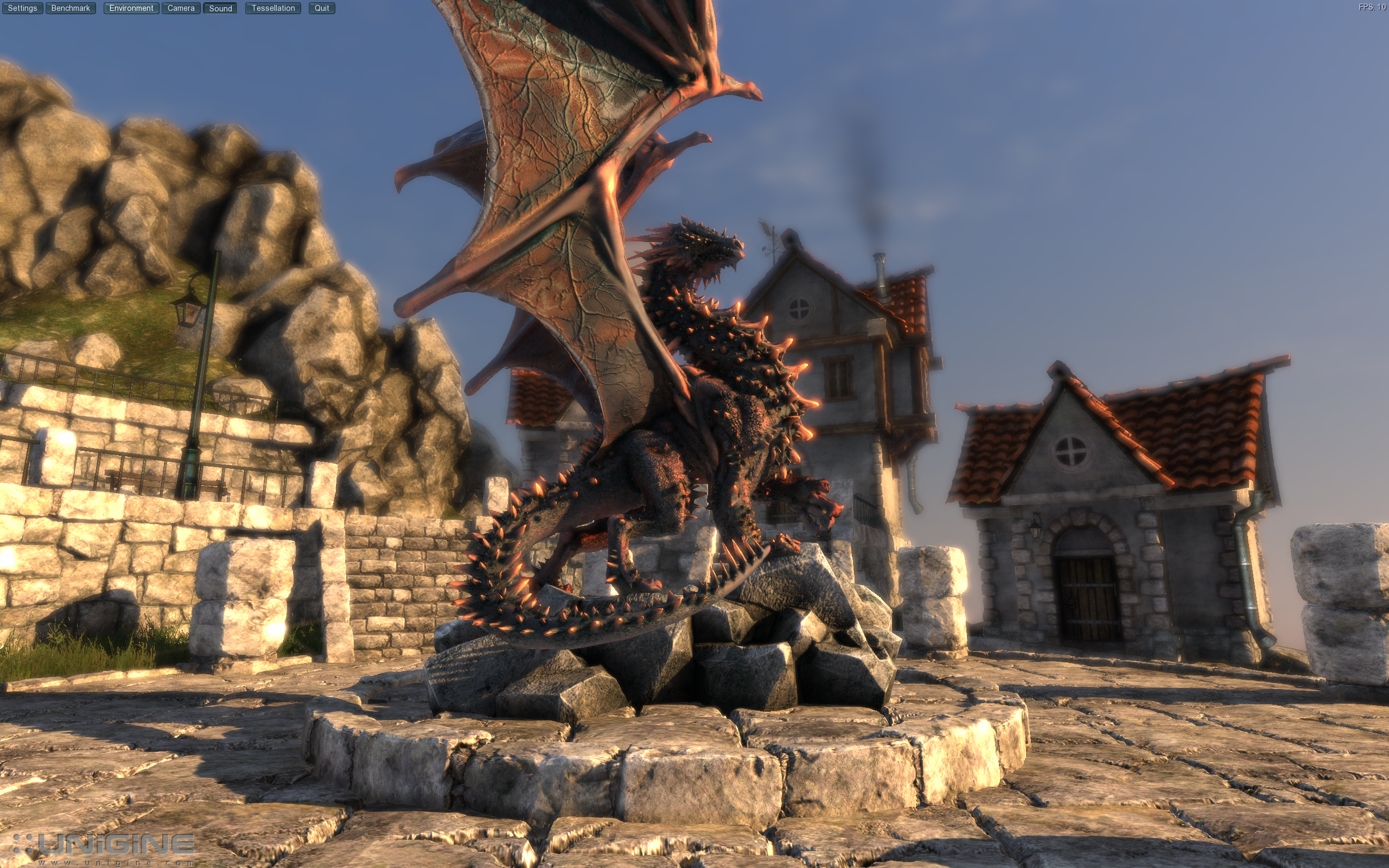
So it’s the third and final change that’s the most interesting. NVIDIA has added a new Transparency Supersampling (TrSS) mode for Fermi (ed: and GT240) that picks up where the old one left off. Their previous TrSS mode only worked on DX9 titles, which meant that users had few choices for anti-aliasing fake geometry under DX10 games. This new TrSS mode works under DX10, it’s as simple as that.
So why is this a big deal? Because a lot of DX10 games have bad aliasing of fake geometry, including some very popular ones. Under Crysis in DX10 mode for example you can’t currently anti-alias the foliage, and even brand-new games such as Battlefield: Bad Company 2 suffer from aliasing. NVIDIA’s new TrSS mode fixes all of this.
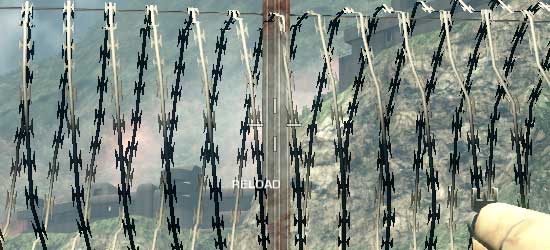
Bad Company 2 DX11 Without Transparency Supersampling
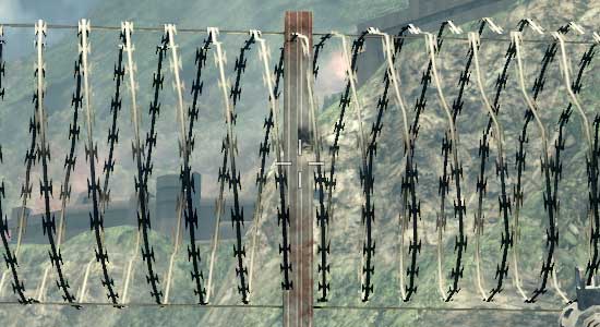
Bad Company 2 DX11 With Transparency Supersampling
The bad news is that it’s not quite complete. Oh as you’ll see in our screenshots it works, but the performance hit is severe. It’s currently super-sampling too much, resulting in massive performance drops. NVIDIA is telling us that this should be fixed next month, at which time the performance hit should be similar to that of the old TrSS mode under DX9. We’ve gone ahead and taken screenshots and benchmarks of the current implementation, but keep in mind that performance should be greatly improving next month.
So with that said, let’s look at the screenshots.
| NVIDIA GeForce GTX 480 | NVIDIA GeForce GTX 285 | ATI Radeon HD 5870 | ATI Radeon HD 4890 |
| 0x | 0x | 0x | 0x |
| 2x | 2x | 2x | 2x |
| 4x | 4x | 4x | 4x |
| 8xQ | 8xQ | 8x | 8x |
| 16xQ | 16xQ | DX9: 4x | DX9: 4x |
| 32x | DX9: 4x | DX9: 4x + AAA | DX9: 4x + AAA |
| 4x + TrSS 4x | DX9: 4x + TrSS | DX9: 4x + SSAA | |
| DX9: 4x | |||
| DX9: 4x + TrSS |
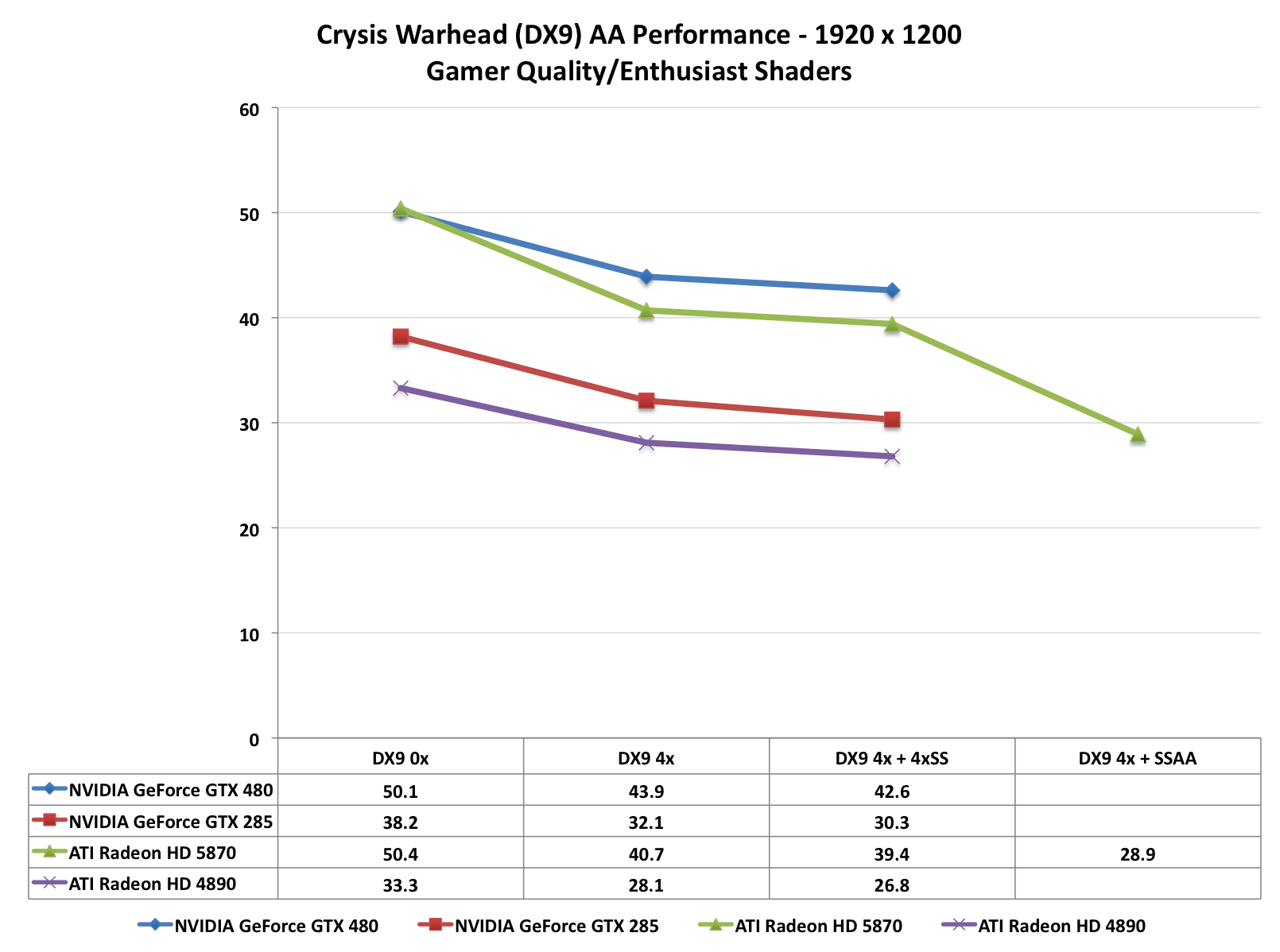
With the exception of NVIDIA’s new TrSS mode, very little has changed. Under DX10 all of the cards produce a very similar image. Furthermore once you reach 4x MSAA, each card producing a near-perfect image. NVIDIA’s new TrSS mode is the only standout for DX10.
We’ve also include a few DX9 shots, although we are in the process of moving away from DX9. This allows us to showcase NVIDIA’s old TrSS mode, along with AMD’s Adapative AA and Super-Sample AA modes. Note how both TrSS and AAA do a solid job of anti-aliasing the foliage, which makes it all the more a shame that they haven’t been available under DX10.
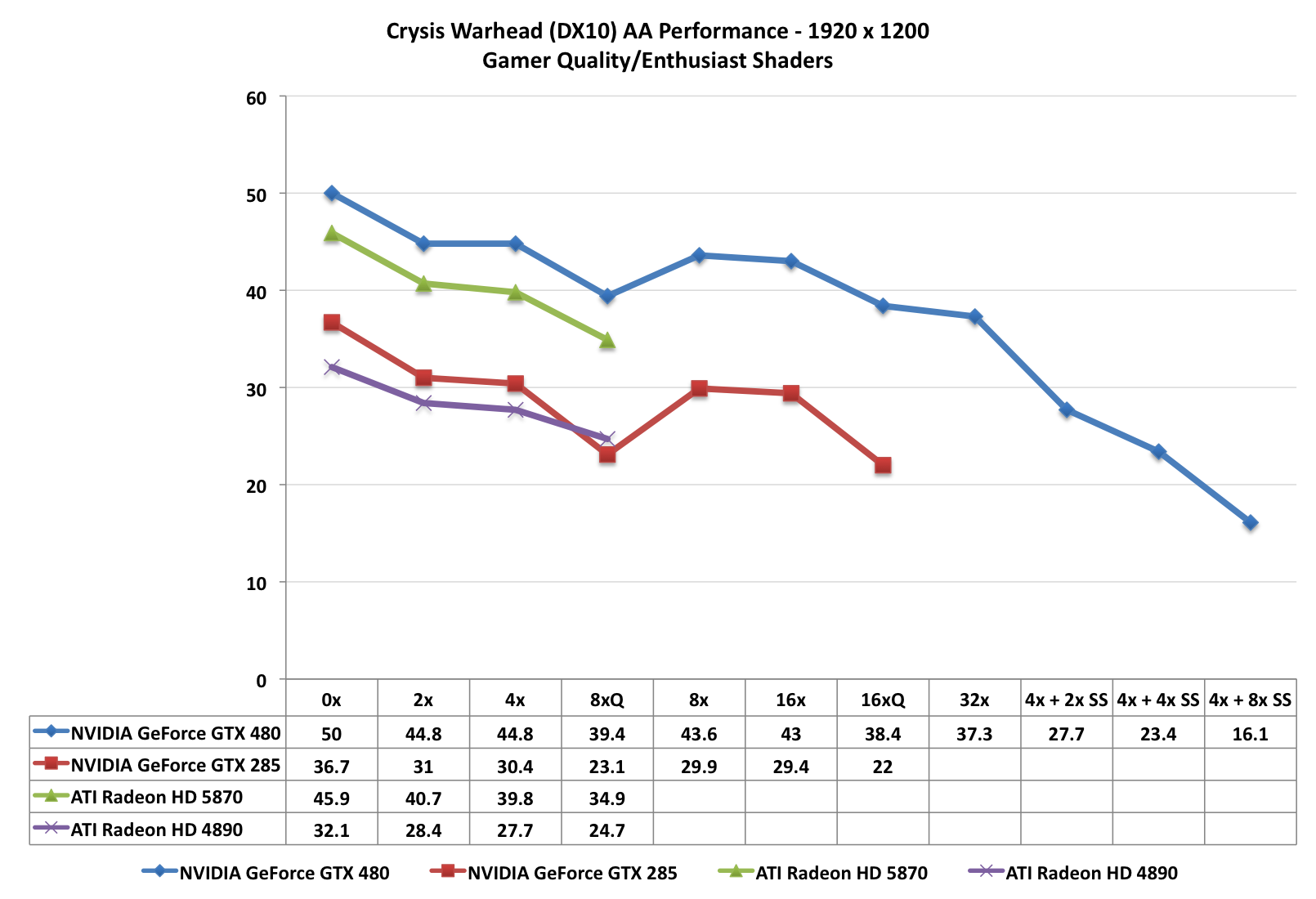
When it comes to performance, keep in mind that both AMD and NVIDIA have been trying to improve their 8x MSAA performance. When we reviewed the Radeon 5870 back in September we found that AMD’s 8x MSAA performance was virtually unchanged, and 6 months later that still holds true. The performance hit moving from 4x MSAA to 8x MSAA on both Radeon cards is roughly 13%. NVIDIA on the other hand took a stiffer penalty under DX10 for the GTX 285, where there it fell by 25%. But now with NVIDIA’s 8x MSAA performance improvements for Fermi, that gap has been closed. The performance penalty for moving to 8x MSAA over 4x MSAA is only 12%, putting it right up there with the Radeon cards in this respect. With the GTX 480, NVIDIA can now do 8x MSAA for as cheap as AMD has been able to
Meanwhile we can see the significant performance hit on the GTX 480 for enabling the new TrSS mode under DX10. If NVIDIA really can improve the performance of this mode to near-DX9 levels, then they are going to have a very interesting AA option on their hands.
Last but not least, there’s anisotropic filtering quality. With the Radeon 5870 we saw AMD implement true angle-independent AF and we’ve been wondering whether we would see this from NVIDIA. The answer is no: NVIDIA’s AF quality remains unchanged from the GTX200 series. In this case that’s not necessarily a bad thing; NVIDIA already had great AF even if it was angle-dependant. More to the point, we have yet to find a game where the difference between AMD and NVIDIA’s AF modes have been noticeable; so technically AMD’s AF modes are better, but it’s not enough that it makes a practical difference
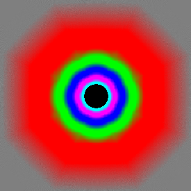
GeForce GTX 480
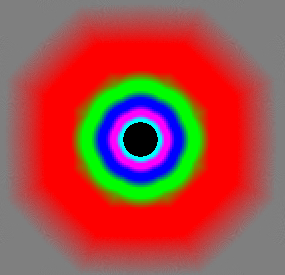
GeForce GTX 285
Radeon 5870
The Test
With the launch of the GTX 400 series, we have gone ahead and completely rebuilt our benchmark suite. This includes rotating out several games for several new games, giving us a nice mix of DX9/10 and DX11 games. Everything else has been rebenchmarked using the latest drivers, and our power data has changed as we installed an Antec 1200W PSUin order to keep up with the potential power demands of a pair of GTX 480s in SLI.
For the AMD cards, we used AMD’s Catalyst 10.3a drivers along with the latest driver profile update. For NVIDIA’s cards NVIDIA supplied us with their Forceware 197.17 drivers, which only work for the GTX 400 series. For the rest of the NVIDIA cards we used the 197.13 drivers.
| CPU: | Intel Core i7-920 @ 3.33GHz |
| Motherboard: | Intel DX58SO (Intel X58) |
| Chipset Drivers: | Intel 9.1.1.1015 (Intel) |
| Hard Disk: | OCZ Summit (120GB) |
| Memory: | Patriot Viper DDR3-1333 3 x 2GB (7-7-7-20) |
| Video Cards: | AMD Radeon HD 5970 AMD Radeon HD 5870 AMD Radeon HD 5850 AMD Radeon HD 5830 AMD Radeon HD 5770 AMD Radeon HD 5750 AMD Radeon HD 4890 AMD Radeon HD 4870 1GB AMD Radeon HD 4850 AMD Radeon HD 3870 NVIDIA GeForce GTX 480 NVIDIA GeForce GTX 470 NVIDIA GeForce GTX 295 NVIDIA GeForce GTX 285 NVIDIA GeForce GTX 275 NVIDIA GeForce GTX 260 Core 216 NVIDIA GeForce 8800 GT |
| Video Drivers: | NVIDIA ForceWare 197.13 NVIDIA ForceWare 197.17 AMD Catalyst 10.3a |
| OS: | Windows 7 Ultimate 64-bit |
Crysis: Warhead
It’s been over 2 years since the release of the original Crysis, and “but can it run Crysis?” is still a common question even today. With a mix of dense foliage, long draw distances, and high quality textures, Crysis is still a game that can bring any machine to its knees, and is our first choice for testing any video card.
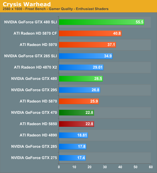
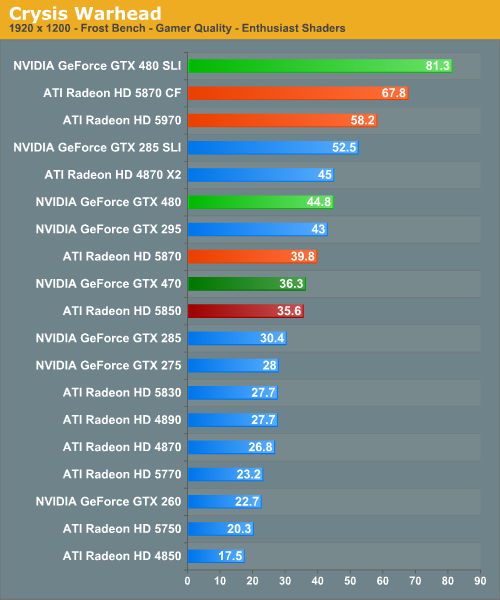
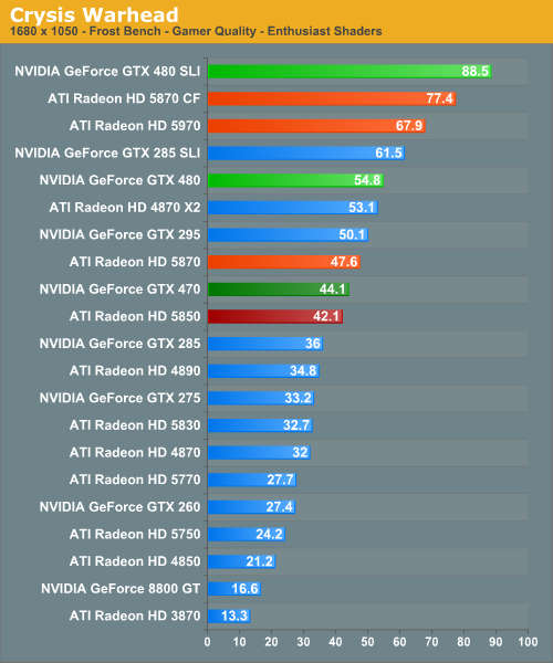
As far as this first game is concerned, things are looking so-so for NVIDIA. For the GTX 480, it’s in a solid 10-12% lead over the 5870, and unsurprisingly losing to the 5970. For the GTX 470 things are less rosy; it basically is breaking even with the 5850. Furthermore there’s an interesting pattern in our averages: the gap between the GTX 400 series and the Radeon 5000 series shrinks with resolution. Keep an eye on this, it’s going to be a repeating pattern.
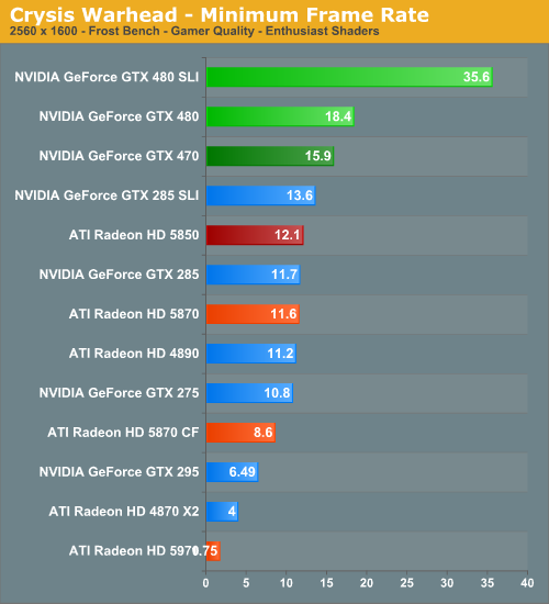
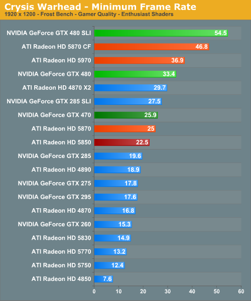
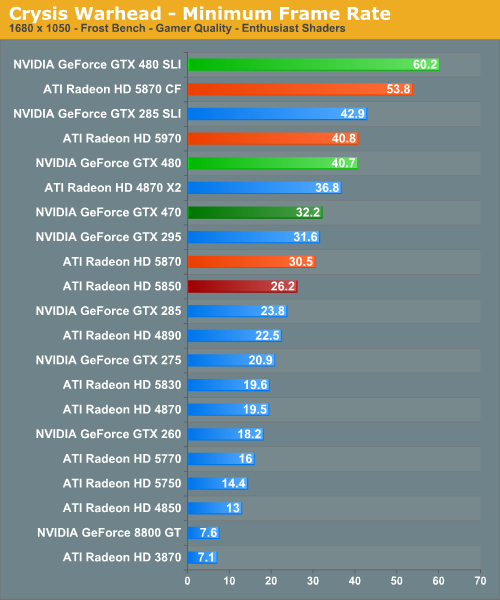
We’ve also gone ahead and recorded the minimum framerates for Crysis, as in our testing we’ve found the minimums to be very reliable. And in doing so, we have some data even more interesting than the averages. The GTX 400 series completely tramples the 5000 series when it comes to minimum framerates, far more than we would have expected. At 2560 Crysis is approaching a video RAM limitation in our 1GB and under cards, which gives the GTX 480 cards a clear lead at those resolutions. But even at lower resolutions where we’re not video RAM limited, the GTX 480 still enjoys a 33% lead in the minimum framerate, and the GTX 470 is well ahead of the 5850 and even slightly ahead of the 5870.
For whatever reason AMD can’t seem to keep up with NVIDIA when it comes to the minimum framerate, even at lower resolutions. Certainly it’s obvious when the 1GB cards are video RAM limited at 2560, but if we didn’t have this data we would have never guessed the minimum framerates were this different at lower resolutions.
Finally we have a quick look at SLI/CF performance. CF seems to exacerbate the video RAM limitations of the 5000 series, resulting in the GTX 480SLI coming in even farther ahead of the 5870CF. Even at lower resolutions SLI seems to be scaling better than CF.
BattleForge: DX10
Up next is BattleForge, Electronic Arts’ free to play online RTS. As far as RTSes go this game can be quite demanding, and this is just at DX10.
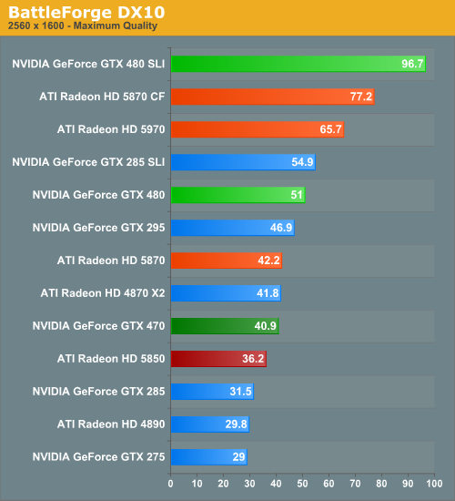
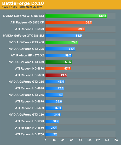
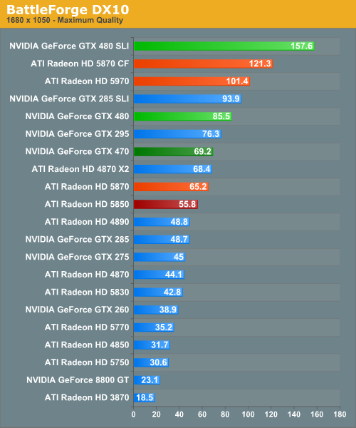
This is another game that treats the GTX 400 series well. The GTX 480 is 20-30% ahead of the Radeon 5870, and the GTX 470 is 12-25% ahead of the 5850. Not surprisingly, the GTX 480SLI is also in a solid lead over the 5870CF.
BattleForge: DX11
While BattleForge can be tough under DX10, under DX11 it’s even more brutal. Here we use the DX11 renderer and turn on self shadowing ambient occlusion (SSAO) to its highest setting, which uses a DX11 ComputeShader.
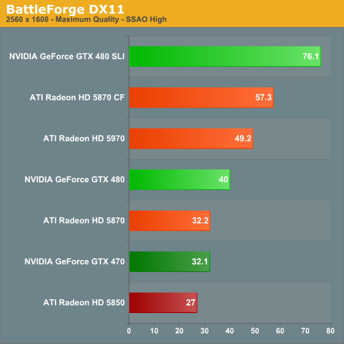

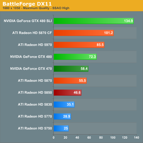
Even with the DX11 ComputeShader, the story remains the same for the GTX 400 series.The GTX 480 enjoys a 20-30% lead, and the GTX 470 takes a smaller 20-25% lead. At this point the GTX 470 is even trading blows with the 5870.
HAWX
Ubisoft’s aerial action game is one of the less demanding games in our benchmark suite, particularly for the latest generation of cards. However it’s fairly unique in that it’s one of the few flying games of any kind that comes with a proper benchmark.

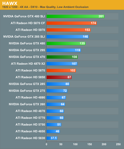
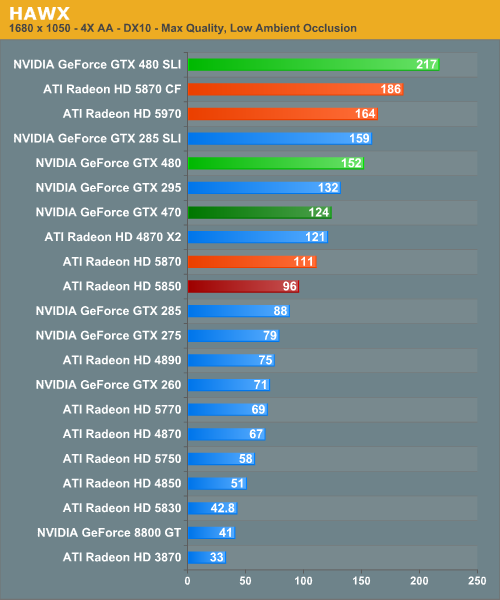
So far, NVIDIA’s leads keep increasing. With HAWX we’re up to a 20-35% lead for the GTX 480, and a 7-30% lead for the GTX 470. On the SLI/CF front however we have a slightly different story. NVIDIA is still in the lead, but their lead ends up shrinking here compared to the more demanding lead a single card has.
Left 4 Dead
Introduced in 2004, Valve’s Source engine continues to live on in new Valve games. At this point even newer Source games like Left 4 Dead are rarely GPU limited to a significant degree, but we keep it on here due to the fact that we’re expecting at least one more Source game this year in Portal 2.
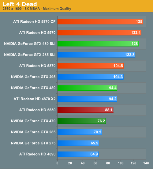
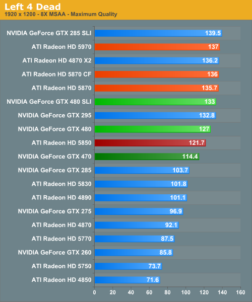
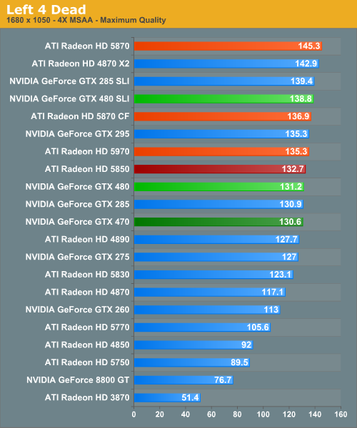
Breaking from tradition a bit, for L4D we’ve gone ahead and cranked up the AA to 8x. The quality difference is tiny at best, but it was necessary to try to keep the GTX 480 and 5870 from getting more than 100fps at 2560 (and it still wasn’t enough for the 5870). With that said we see a dramatic reversal from HAWX – the GTX 400 series loses its first game. The GTX 480 falls behind by 6-9% while the GTX 470 falls behind by anywhere between 1 and 15%. Interestingly on the GTX 470 in particular, the gap grows with resolution; perhaps we’re seeing the ROP loss come to haunt us?
In any case, if you’re going to lose a game, L4D is not a bad game to lose at. Even the GTX 275 gets over 60fps at 2560, so while it’s a loss on paper there’s little practical difference..
Battlefield: Bad Company 2
The latest game in the Battlefield series - Bad Company 2 - is another one of our new DX11 games and has been a smash hit at retail. It’s also surprisingly hard on our GPUs, enough so that we can say we found something that’s more demanding than Crysis. As BC2 doesn’t have a built-in benchmark or recording mode, here we take a FRAPS run of the jeep chase in the first act, which as an on-rails portion of the game provides very consistent results and a spectacle of explosions, trees, and more.
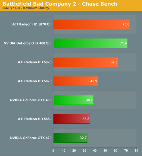
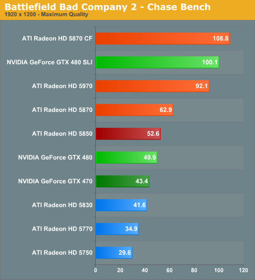
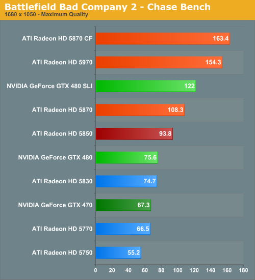
Unfortunately for NVIDIA this is another losing game for them, and at times they lose big. The GTX 480 comes in at 20% behind the 5870 at 1920, while the GTX 470 comes in behind the 5850 by a similar degree at the same resolution. Interestingly we’re once again seeing a narrowing of the gap as resolutions increase – at 2560, it’s a 9%/7% gap respectively. Given the popularity of the game this really isn’t a game you want to be losing at, particularly by double-digit percentages at 1920.
As FRAPSing the chase scene in BC2 doesn’t provide us with a suitable degree of reliability for minimum framerates, we have gone ahead and engineered our own test for minimum framerates. In the 3rd act there is a waterfall that we have found to completely kill the framerate on even the fastest systems, and in play testing we have found that this isn’t too far off from the minimum framerates we find in multiplayer games. So we’re going to use this waterfall test as a stand-in for minimum framerates on BC2.
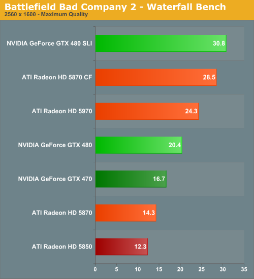
Even with a pair of cards in SLI or Crossfire, at 2560 it’s a struggle to stay above 30fps, with only the GTX 480 SLI regining supreme. In fact the performance on this benchmark is quite different from our earlier benchmark all around. Instead of losing the GTX 400 series wins in a big way - a 9% loss in the chase is a 42% lead for the GTX 480 here, and the 470 attains a 35% lead. At first glance we don’t believe that this is a video RAM limitation like we saw in Crysis, but we’re going to have to wait for AMD to ship their 2GB 5870s before we can fully rule that out.
In the mean time it looks like we have two different outcomes: the Radeon 5000 series has the better average framerate (particularly at 1920), but it’s the GTX 400 series that has the better minimum framerate. If you absolutely can’t stand a choppy minimum framerate, then you may be better off with a GTX 400 card so that you can trade some overall performance for a better minimum framerate.
STALKER: Call of Pripyat
The 3rd game in the STALKER series continues to build on GSC Game World’s X-Ray Engine by adding DX11 support, tessellation, and more. This also makes it another one of the highly demanding games in our benchmark suite.
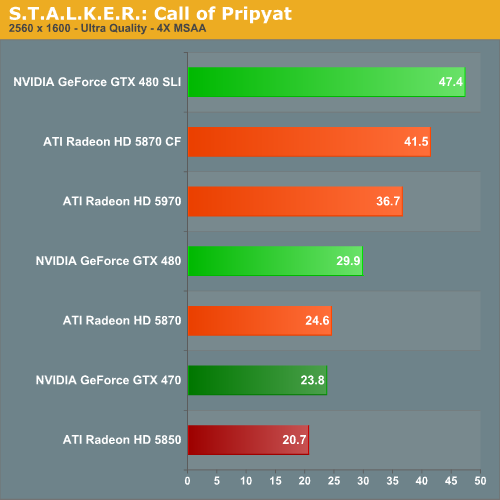
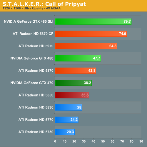
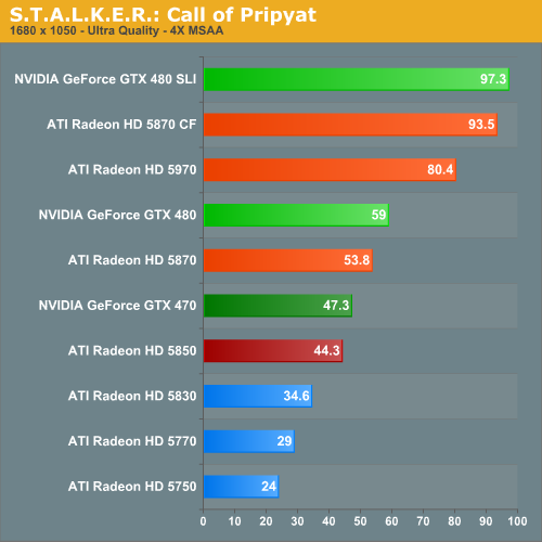
After losing in Left 4 Dead and Bad Company 2, the GTX 400 series is back in the winner’s circle here, and once again by double-digit percentages. In fact the situation is quite unusual – the higher the resolution, the wider the gap gets. At any rate, no single GPU is powerful enough to hit a playable framerate under STALKER at 2560 – here you have to go multi-GPU if you wish to break 30fps at the highest settings at the highest resolutions.
DIRT 2
Codemasters latest racing game marks the return of a racer to our benchmark suite. As the first DX11 racer, DIRT 2 makes pretty through use of the DX11’s tessellation abilities, not to mention being the best looking racer we have ever seen.
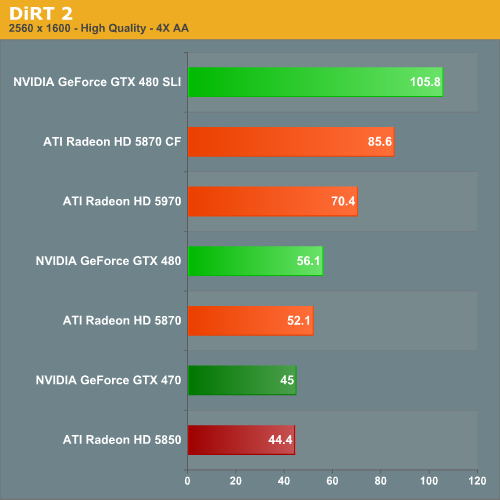
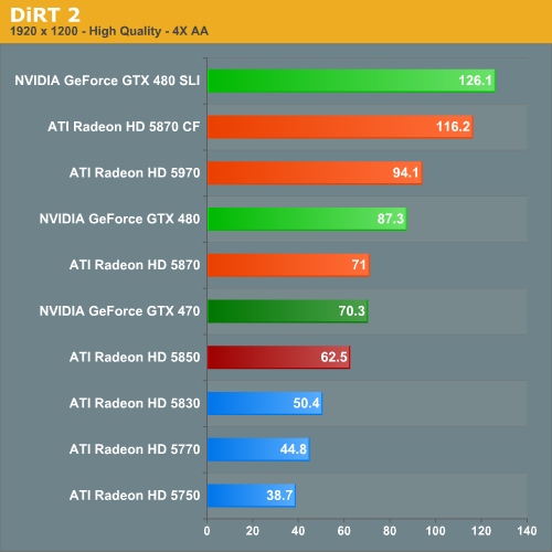
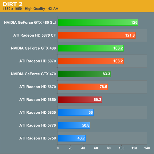
DIRT 2 may have started life as an AMD sponsored game, but here it’s all about NVIDIA. The GTX 480 wins by 7-31%, and the 470 by anywhere from 1 to 20%. Once again we’re seeing the gap close with resolution, with the GeForces and Radeons only barely separated at 2560. SLI/CF scaling is a different story though; until 2560, CF scales better than SLI, leading to only a small gap between the GTX 480SLI and 5870CF at 1920.
Mass Effect 2
Electronic Arts’ recently released space-faring RPG is our new Unreal Engine 3 game. While it doesn’t have a built in benchmark, it does let us force anti-aliasing through driver control panels, giving us a better idea of UE3’s performance at higher quality settings. Since we can’t use a recording/benchmark in ME2, we use FRAPS to record a short run.
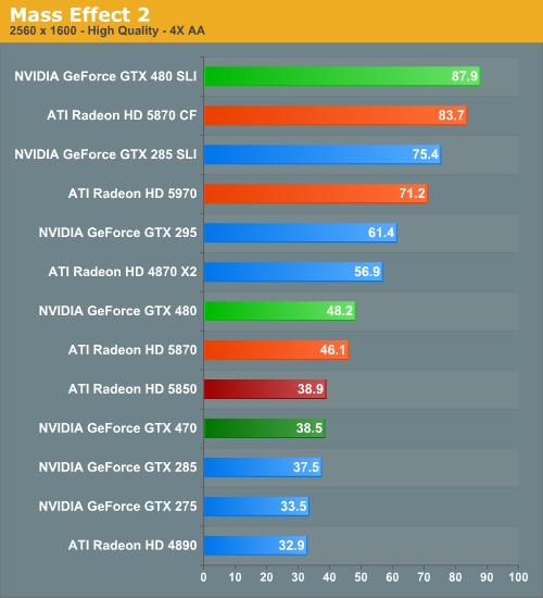
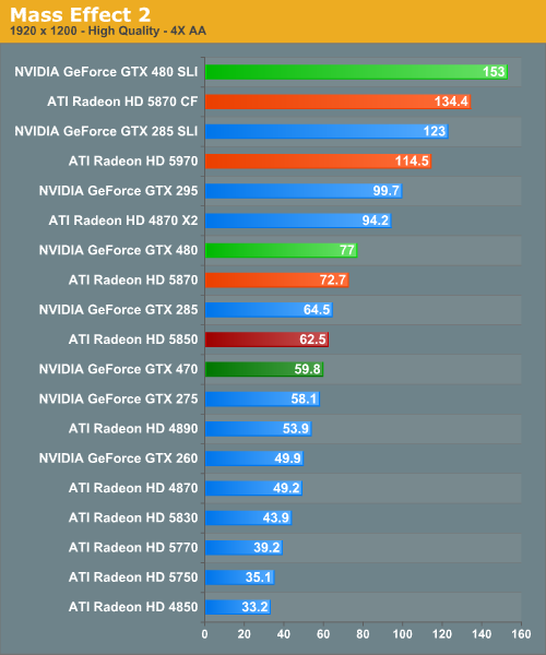
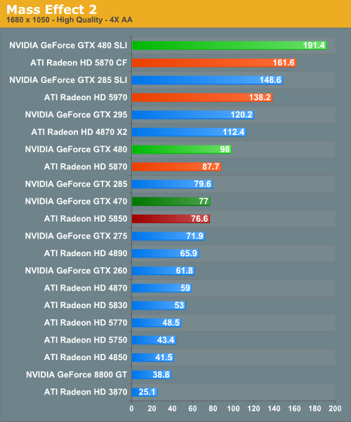
ME2 is another victory for NVIDIA, albeit the smallest one we’ve yet to see. Here the GTX 480 is 4-11% ahead, while the 5850 and GTX 470 are tangled among each other the entire way. Meanwhile we once again see what little performance gap exists between the GTX 480 and 5870 dissipate as we increase the resolution.
Wolfenstein
Finally among our revised benchmark suite we have Wolfenstein, the most recent game to be released using the id Software Tech 4 engine. All things considered it’s not a very graphically intensive game, but at this point it’s the most recent OpenGL title available. It’s more than likely the entire OpenGL landscape will be thrown upside-down once id releases Rage later this year.
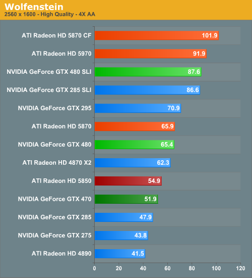
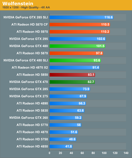
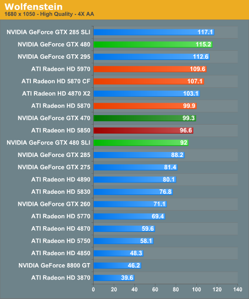
The most distinguishing result in this benchmark is that it once again shows the Radeon and GeForce performance gap closing with resolution, with the GTX 480 going from a 15% lead to a fraction of a percentage loss by the time we reach 2560. The GTX 470 shares a similar story, however it ends up with a more definite loss by the end. Given the framerates we’re seeing at 1680, it’s likely that we’re CPU limited and are seeing driver overhead come in to play.
Temperature, Power, & Noise: Hot and Loud, but Not in the Good Way
For all of the gaming and compute performance data we have seen so far, we’ve only seen half of the story. With a 500mm2+ die and a TDP over 200W, there’s a second story to be told about the power, temperature, and noise characteristics of the GTX 400 series.
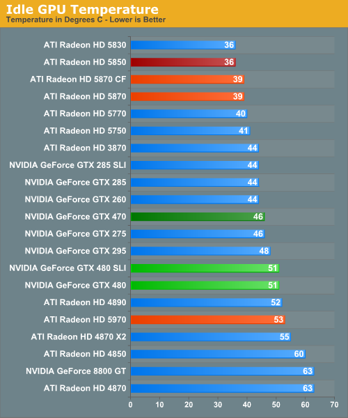
Starting with idle temperatures, we can quickly see some distinct events among our cards. The top of the chart is occupied solely by AMD’s Radeon 5000 series, whose small die and low idle power usage let these cards idle at very cool temperatures. It’s not until half-way down the chart that we find our first GTX 400 card, with the 470 at 46C. Truth be told we were expecting something a bit better out of it given that its 33W idle is only a few watts over the 5870 and has a fairly large cooler to work with. Farther down the chart is the GTX 480, which is in the over-50 club at 51C idle. This is where NVIDIA has to pay the piper on their die size – even the amazingly low idle clockspeed of 50MHz/core 101MHz/shader 67.5Mhz/RAM isn't enough to drop it any further.
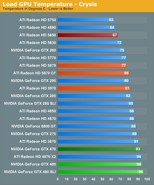
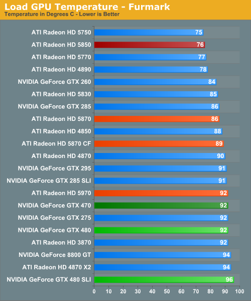
For our load temperatures, we have gone ahead and added Crysis to our temperature testing so that we can see both the worst-case temperatures of FurMark and a more normal gameplay temperature.
At this point the GTX 400 series is in a pretty exclusive club of hot cards – under Crysis the only other single-GPU card above 90C is the 3870, and the GTX 480 SLI is the hottest of any configuration we have tested. Even the dual-GPU cards don’t get quite this hot. In fact it’s quite interesting that unlike FurMark there’s quite a larger spread among card temperatures here, which only makes the GTX 400 series stand out more.
While we’re on the subject of temperatures, we should note that NVIDIA has changed the fan ramp-up behavior from the GTX 200 series. Rather than reacting immediately, the GTX 400 series fans have a ramp-up delay of a few seconds when responding to high temperatures, meaning you’ll actually see those cards get hotter than our sustained temperatures. This won’t have any significant impact on the card, but if you’re like us your eyes will pop out of your head at least once when you see a GTX 480 hitting 98C on FurMark.
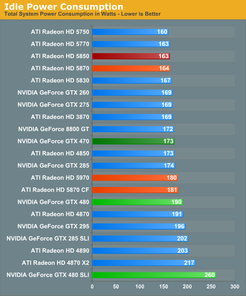
Up next is power consumption. As we’ve already discussed, the GTX 480 and GTX 470 have an idle power consumption of 47W and 33W respectively, putting them out of the running for the least power hungry of the high-end cards. Furthermore the 1200W PSU we switched to for this review has driven up our idle power load a bit, which serves to suppress some of the differences in idle power draw between cards.
With that said the GTX 200 series either does decently or poorly, depending on your point of view. The GTX 480 is below our poorly-idling Radeon 4000 series cards, but well above the 5000 series. Meanwhile the GTX 470 is in the middle of the pack, sharing space with most of the GTX 200 series. The lone outlier here is the GTX 480 SLI. AMD’s power saving mode for Crossfire cards means that the GTX 480 SLI is all alone at a total power draw of 260W when idle.
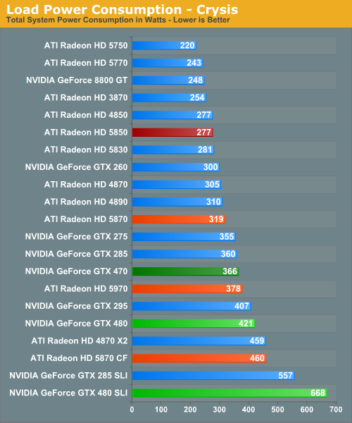
For load power we have Crysis and FurMark, the results of which are quite interesting. Under Crysis not only is the GTX 480 SLI the most demanding card setup as we would expect, but the GTX 480 itself isn’t too far behind. As a single-GPU card it pulls in more power than either the GTX 295 or the Radeon 5970, both of which are dual-GPU cards. Farther up the chart is the GTX 470, which is the 2nd most power draining of our single-GPU cards.
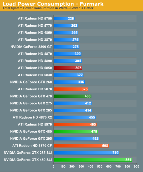
Under FurMark our results change ever so slightly. The GTX 480 manages to get under the GTX 295, while the GTX 470 falls in the middle of the GTX 200 series pack. A special mention goes out to the GTX 480 SLI here, which at 851W under load is the greatest power draw we have ever seen for a pair of GPUs.
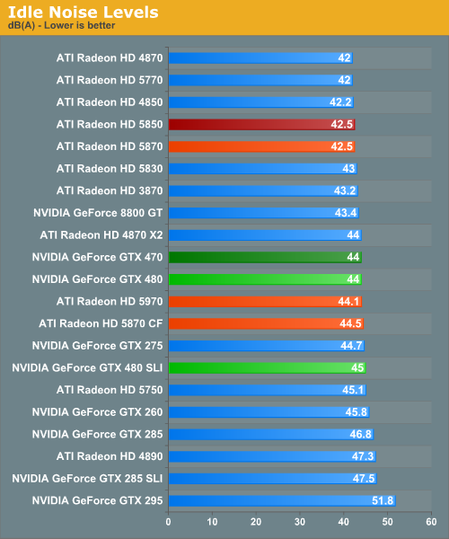
Idle noise doesn’t contain any particular surprises since virtually every card can reduce its fan speed to near-silent levels and still stay cool enough. The GTX 400 series is within a few dB of our noise floor here.
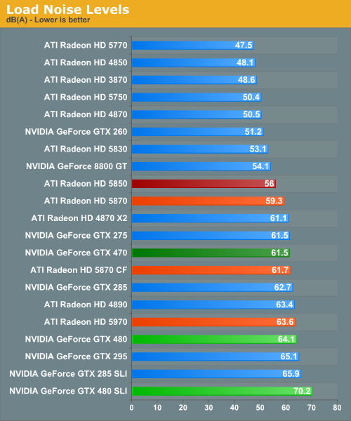
Hot, power hungry things are often loud things, and there are no disappointments here. At 70dB the GTX 480 SLI is the loudest card configuration we have ever tested, while at 64.1dB the GTX 480 is the loudest single-GPU card, beating out even our unreasonably loud 4890. Meanwhile the GTX 470 is in the middle of the pack at 61.5dB, coming in amidst some of our louder single-GPU cards and our dual-GPU cards.
Finally, with this data in hand we went to NVIDIA to ask about the longevity of their cards at these temperatures, as seeing the GTX 480 hitting 94C sustained in a game left us worried. In response NVIDIA told us that they have done significant testing of the cards at high temperatures to validate their longevity, and their models predict a lifetime of years even at temperatures approaching 105C (the throttle point for GF100). Furthermore as they note they have shipped other cards that run roughly this hot such as the GTX 295, and those cards have held up just fine.
At this point we don’t have any reason to doubt NVIDIA’s word on this matter, but with that said this wouldn’t discourage us from taking the appropriate precautions. Heat does impact longevity to some degree – we would strongly consider getting a lifetime warranty for the GTX 480 to hedge our bets.
Final Words
To wrap things up, let’s start with the obvious: NVIDIA has reclaimed their crown – they have the fastest single-GPU card. The GTX 480 is between 10 and 15% faster than the Radeon 5870 depending on the resolution, giving it a comfortable lead over AMD’s best single-GPU card.
With that said, we have to take pause for a wildcard: AMD’s 2GB Radeon 5870, which will be launching soon. We know the 1GB 5870 is RAM-limited at times, and while it’s unlikely more RAM on its own will be enough to make up the performance difference, we can’t fully rule that out until we have the benchmarks we need. If the GTX 480 doesn’t continue to end up being the fastest single-GPU card out there, we’ll be surprised.
The best news in this respect is that you’ll have time to soak in the information. With a retail date of April 12th, if AMD launches their card within the next couple of weeks you’ll have a chance to look at the performance of both cards and decide which to get without getting blindsided.
On a longer term note, we’re left wondering just how long NVIDIA can maintain this lead. If a 2GB Radeon isn’t enough to break the GTX 480, how about a higher clocked 5800 series part? AMD has had 6 months to refine and respin as necessary; with their partners already producing factory overclocked cards up to 900MHz, it’s too early to count AMD out if they really want to do some binning in order to come up with a faster Radeon 5800.
Meanwhile let’s talk about the other factors: price, power, and noise. At $500 the GTX 480 is the world’s fastest single-GPU card, but it’s not a value proposition. The price gap between it and the Radeon 5870 is well above the current performance gap, but this has always been true about the high-end. Bigger than price though is the tradeoff for going with the GTX 480 and its much bigger GPU – it’s hotter, it’s noisier, and it’s more power hungry, all for 10-15% more performance. If you need the fastest thing you can get then the choice is clear, otherwise you’ll have some thinking to decide what you want and what you’re willing to live with in return.
Moving on, we have the GTX 470 to discuss. It’s not NVIDIA’s headliner so it’s easy to get lost in the shuffle. With a price right between the 5850 and 5870, it delivers performance right where you’d expect it to be. At 5-10% slower than the 5870 on average, it’s actually a straightforward value proposition: you get 90-95% of the performance for around 87% of the price. It’s not a huge bargain, but it’s competitively priced against the 5870. Against the 5850 this is less true where it’s a mere 2-8% faster, but this isn’t unusual for cards above $300 – the best values are rarely found there. The 5850 is the bargain hunter’s card, otherwise if you can spend more pick a price and you’ll find your card. Just keep in mind that the GTX 470 is still going to be louder/hotter than any 5800 series card, so there are tradeoffs to make, and we imagine most people would err towards the side of the cooler Radeon cards.
With that out of the way, let’s take a moment to discuss Fermi’s future prospects. Fermi’s compute-heavy and tessellation-heavy design continues to interest us but home users won’t find an advantage to that design today. This is a card that bets on the future and we don’t have our crystal ball. With some good consumer-oriented GPGPU programs and developers taking up variable tessellation NVIDIA could get a lot out of this card, or if that fails to happen they could get less than they hoped for. All we can do is sit and watch – it’s much too early to place our bets.
As for NVIDIA’s ecosystem, the situation hasn’t changed much from 2009. NVIDIA continues to offer interesting technologies like PhysX, 3D Vision, and CUDA’s wider GPGPU application library. But none of these are compelling enough on their own, they’re merely the icing on the cake. But if you’re already in NVIDIA’s ecosystem then the choice seems clear: NVIDIA has a DX11 card ready to go that lets you have your cake and eat it too.
Finally, as we asked in the title, was it worth the wait? No, probably not. A 15% faster single-GPU card is appreciated and we’re excited to see both AMD and NVIDIA once again on competitive footing with each other, but otherwise with much of Fermi’s enhanced abilities still untapped, we’re going to be waiting far longer for a proper resolution anyhow. For now we’re just happy to finally have Fermi, so that we can move on to the next step.


I'll bookmark this one. thanks! http://install-how.blogspot.com/2010/06/coretemps-realtemps-and-intelburntest.html
ReplyDelete